In recent years, conformal electronic circuits integrated onto curved surfaces have garnered significant attention due to their wide-ranging applications in health monitoring and diagnostics, motion sensing, wearable devices, antennas, and optoelectronic components.
Additive manufacturing technology enables printing directly onto curved surfaces, offering greater flexibility in circuit design and superior adaptability to complex surface topologies. By employing an innovative electrohydrodynamic (EHD) printing strategy, conductive circuits with micrometer-scale resolution and high uniformity can be printed directly onto various curved surfaces.
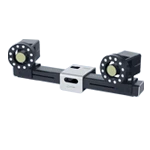
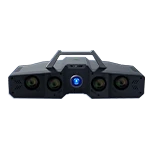
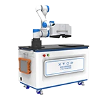
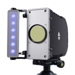
Using the XTOP3D XTOM high-precision blue-light 3D scanner, 3D point cloud data representing the surface morphology can be acquired from high-quality scans. Leveraging this data to adjust printing parameters based on surface curvature facilitates the uniform EHD printing of conductive patterns—with a line width of 39.31 ± 4.06 micrometers—across surfaces with curvatures ranging from 10 to 2000 m⁻¹.
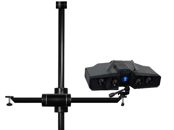
The XTOM high-precision blue-light 3D scanner enables the efficient acquisition of 3D point cloud data from free-form surfaces; this data serves as the basis for subsequent design of conductive features and path planning using Python-based software. By integrating blue-light 3D scanning, path planning, and speed-adaptive electro-hydrodynamic printing, conductive circuits with micrometer-scale resolution and high uniformity can be printed directly onto various curved surfaces.
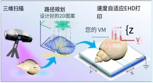
Existing technologies, such as inkjet or extrusion printing, are unable to deposit micro-scale conductive circuits that conform to complex, free-form surfaces with varying curvature.
1. An innovative electrohydrodynamic (EHD) printing strategy is employed to adaptively adjust the nozzle-to-substrate distance and printing speed based on surface curvature, enabling the direct printing of highly uniform conductive circuits with micro-scale resolution onto various free-form surfaces.
2. A path-planning algorithm was developed to determine printing trajectories based on surface curvature variations, thereby achieving high-precision printing of conductive circuits on complex surfaces.
As a proof of concept, a uniform snowflake pattern with excellent electrical conductivity was printed via EHD onto a naturally insulating conch shell, achieving a minimum linewidth of 35.74 ± 4.24 micrometers.
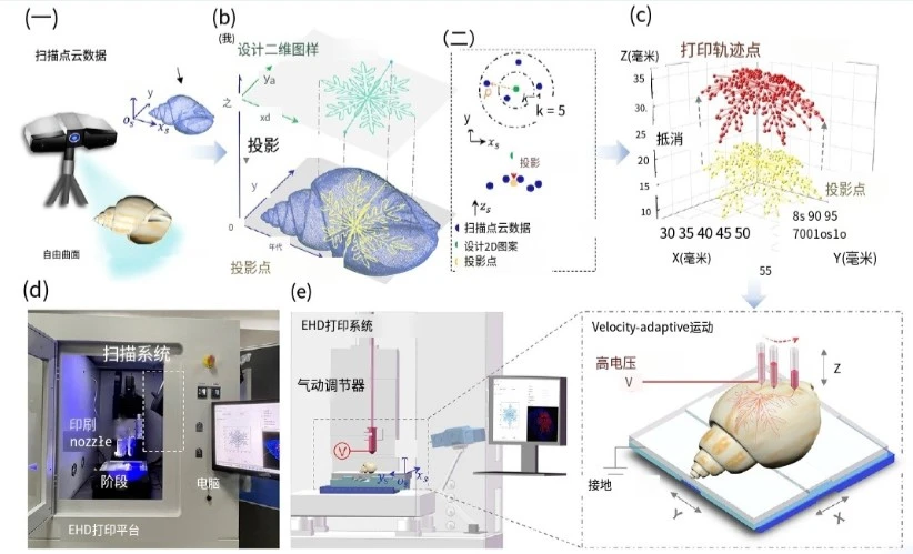
Figure 1. Flowchart of 3D path planning and platform setup for conformal EHD printing on various curved surfaces.
(a) 3D scanning of a free-form surface to acquire point cloud data representing the target surface geometry. (b) Schematic illustrating the projection of a designed 2D pattern onto the target surface using the KNN algorithm to obtain corresponding projected 3D points (i) and (ii). (c) Offsetting the projected points to generate trajectory points for EHD printing. (d) Conformal EHD printing platform and (e) schematic of the adaptive-speed conformal EHD printing strategy for fabricating conductive patterns on a conch shell surface.
3D Path Planning for Conformal EHD Printing on Freeform Surfaces
Path planning is crucial for establishing the link between the surface information of a 3D model—obtained via an XTOM blue-light 3D scanner—and the actual printing trajectory during the EHD manufacturing process.
The figure above illustrates the key steps of conformal EHD printing on freeform surfaces, involving 3D scanning and path planning.
1. Use the XTOM high-precision blue-light 3D scanner to rapidly capture the geometry of the target surface (i.e., the substrate).
2. Convert the scanned surface data into 3D point cloud data to represent the substrate's surface information within a projected 3D coordinate system.
3. Construct a 2D plane above the scanned model and define a 2D pattern using a set of discrete points; project these points onto the surface using the KNN algorithm, and adjust parameters to map the 2D data to the surface coordinates.
4. Apply an offset to the projected points to generate the final printing trajectory points, serving as the path for conformal EHD printing on various substrates. The conformal EHD printing platform prints complex freeform helical patterns onto diverse substrates.
Optimizing Process Parameters to Enhance EHD Printing Precision
Optimizing process parameters—such as the number of projected points and the KNN algorithm parameters used for path planning—is essential for ensuring the precision and efficiency of Electrohydrodynamic (EHD) printing.
1. Utilize the XTOM high-precision blue-light 3D scanner to acquire a high-density point dataset (as the training set) and use the designed 2D pattern points (as the test set) to train the KNN algorithm for optimization within the printing path planning process.
2. Employ blue-light 3D scanning technology to acquire point cloud data; optimize the number of projected points along the scanning path to enhance pattern fidelity and the stability of the moving platform.
3. Optimize the threshold parameters for EHD printing on the surface; this enabled the printing of continuous, high-fidelity snowflake patterns at a constant printing speed of 10 mm/s.
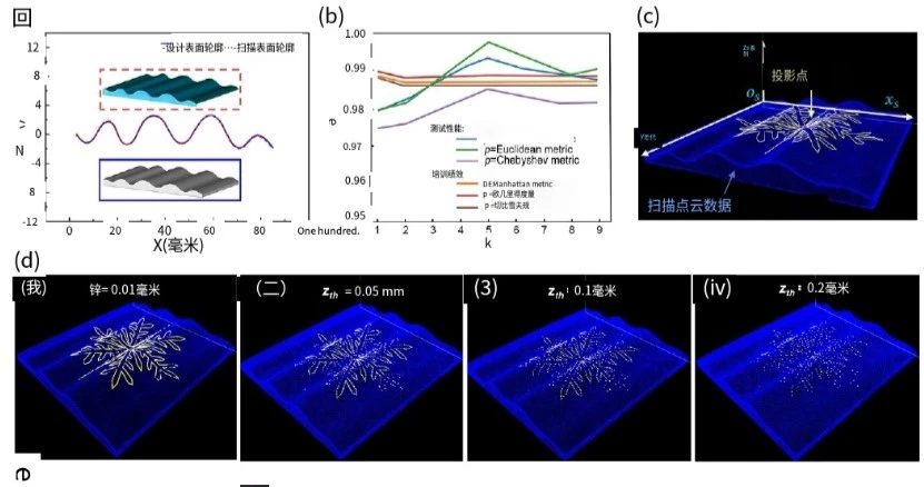
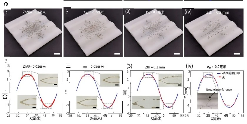
Figure 2. Optimization of projected data within the selected threshold-based path planning algorithm to enable high-fidelity EHD printing of patterns on freeform surfaces while maintaining the stability of the mobile platform.
(a) Comparison between the designed and scanned target surface profiles. (b) Accuracy comparison of testing and training performance using different metrics. (c) Projected points for a snowflake pattern obtained via the optimized KNN algorithm. (d) Projected points of the printing path at different threshold settings. (e) EHD-printed snowflake patterns at four different threshold levels. (f) Adaptability of trajectory points to the surface at four different threshold levels. Scale bar: 1 mm.
In the field of electronic printing, 3D scanning technology is primarily combined with the Direct Ink Writing (DIW) process to fabricate conformal circuits on curved surfaces; however, circuits produced via DIW typically exhibit resolutions coarser than 1 millimeter. In contrast, combining 3D scanning with Direct Laser Writing enables the fabrication of conformal circuits with line widths as fine as 100 micrometers.
By integrating a high-precision XTOM blue-light 3D scanner with an electro-hydrodynamic printing system featuring path planning and adaptive speed control, conductive circuits with micrometer-scale resolution and high uniformity can be printed directly onto diverse curved surfaces. Further advancements in electro-hydrodynamic jet printing technology promise to simplify the manufacturing process for curved functional devices, paving the way for sophisticated 3D electronic devices capable of complex functions, such as electromagnetic modulation.
Case study excerpted from: [Yue Junyu, State Key Laboratory of Manufacturing Systems Engineering, Xi'an Jiaotong University: Flow-Rate-Adaptive Electrohydrodynamic Jet Printing Technology for Conformal Micro-Scale Circuits on Free-Form Surfaces]