Abstract
During semiconductor manufacturing and chip packaging, thermal warpage in wafers is a critical factor triggering issues such as chip cracking, open circuits at solder joints, electrical shorts, device performance drift, and even total system failure. Leveraging the advantages of non-contact, full-field, and micron-level measurement, Digital Image Correlation (DIC) technology—specifically 3D strain measurement systems—can capture comprehensive data on 3D warpage morphology, displacement fields, and strain fields across the entire temperature range. This provides a quantitative basis for optimizing wafer processes, designing for thermal matching in packaging, and certifying the reliability of automotive-grade chips.
This article focuses on the XTOP3D XTDIC-CONST 3D DIC strain measurement system, detailing the application background, technical comparisons, system configuration, key technical challenges, and actual measurement case studies regarding wafer thermal warpage testing.
I. Application Background: The Impact of Wafer Thermal Warpage on Semiconductor Devices
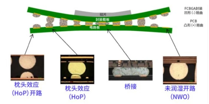
Testing for thermal deformation in wafers is a core procedure in the R&D, manufacturing, and packaging/testing stages of semiconductor production. Differences in the Coefficient of Thermal Expansion (CTE) among the various materials within a chip make wafers highly susceptible to warpage and localized cracking during processes such as high-temperature deposition, etching, and reflow soldering, as well as during actual device operation. These issues can lead to soldering failures—such as "Head-on-Pillow" (HoP) open circuits, bridging, and non-wetting—ultimately resulting in severe quality problems, including electrical shorts, performance drift, and total chip failure.
DIC 3D full-field strain measurement finds applications across the entire semiconductor industry chain, including the characterization of thermal deformation during high-temperature wafer processing, reliability verification of 3C electronics in extreme environments, AEC-Q100 certification testing for automotive chips, and long-term high-temperature service risk assessment for 5G base station and high-performance computing chips. By accurately capturing data on wafer thermal warpage, full-field displacement, and thermal strain, the technology enables the early prediction of thermal deformation trends, supports the optimization of chip structures and packaging designs, and helps reduce product scrap rates.
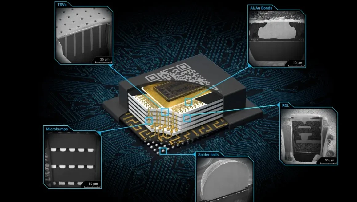
Schematic diagram of the chip packaging structure
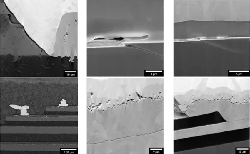
Thermal deformation-induced fracture surfaces of various types of failure
II. Measurement Principle of DIC (Digital Image Correlation) Technology
DIC technology (specifically 3D DIC) integrates binocular stereo vision with close-range photogrammetry algorithms. By tracking speckle features on the specimen surface and comparing changes in speckle positions between reference and deformed images, the system calculates 3D coordinates, full-field displacement, and strain distribution, thereby enabling non-contact, quantitative deformation measurement.
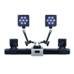
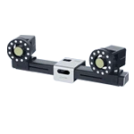
The XTDIC-CONST 3D DIC strain measurement system operates on this principle, providing visual output of surface deformation under both static and dynamic conditions. It is ideally suited for testing and analyzing minute thermal warpage in microelectronic components such as wafers, PCBs, and chip packages.
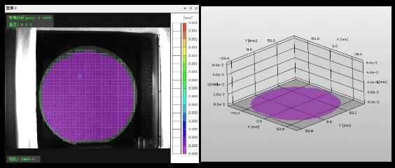
Schematic diagram of wafer thermal deformation measurement and analysis
III. Comparison of Mainstream Wafer Thermal Deformation Testing Technologies
Currently, the industry primarily employs three methods for wafer deformation detection: 3D full-field strain measurement using Digital Image Correlation (DIC), White Light Interferometry (WLI), and resistance strain gauges. These technologies differ significantly in terms of measurement methodology, data dimensionality, and measurement accuracy.
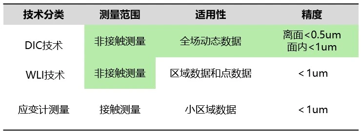
Compared to other methods, the 3D DIC strain measurement system offers sub-pixel resolution, non-contact and non-destructive operation, comprehensive full-field analysis, real-time data output, and strong adaptability to various operating conditions. It provides both quantitative numerical data and intuitive visualizations of strain field distributions, making it a highly efficient tool for testing thermal warpage and the coefficient of thermal expansion (CTE) in semiconductor wafers.
IV. 3D DIC Strain Measurement System Test Setup
4.1 System Hardware Configuration
The complete wafer thermal warpage DIC measurement system consists of a TDIC-CONST 3D full-field strain measurement head, a high-low temperature test chamber, and a temperature controller. The test chamber operates within a temperature range of -40°C to 200°C and features an optical viewing window at the top; the binocular DIC measurement head is positioned outside the chamber, capturing images of the wafer specimen inside through the window. The temperature controller feeds real-time temperature signals into the DIC analysis software, enabling the synchronized and automated acquisition of temperature and image data.
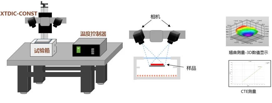
Schematic of the DIC strain measurement system structure, test optical path, and output.
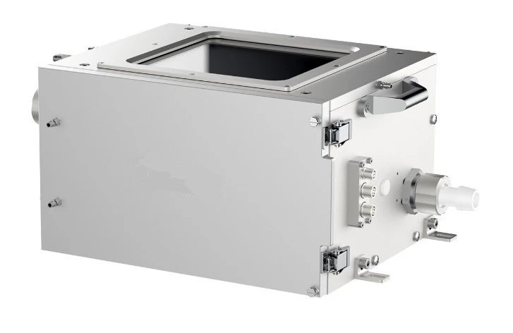
High and Low Temperature Test Chamber
Applications: Microelectronic samples such as silicon wafers, packaged wafers, BGA chips, substrates, and film frames; capable of measuring thermal warpage, coplanarity, full-field strain, and the coefficient of thermal expansion (CTE).
4.2 Key Challenges and Specialized Technologies for DIC Measurement under High-Temperature Conditions
When standard DIC equipment is used directly to test wafers inside a sealed thermal chamber, it encounters two major sources of interference: rigid-body displacement and optical distortion caused by the viewing window. The XTDIC-CONST 3D full-field strain measurement system employs specialized algorithms to eliminate these errors:
1. Rigid-Body Displacement Elimination Algorithm
Fixtures and stages inside the thermal chamber undergo thermal expansion and contraction as the temperature changes, causing the sample to undergo overall rigid-body motion that masks the wafer's actual warpage and deformation. Rigid-body displacement elimination technology is used to filter out the overall displacement caused by the tooling, isolating and retaining only the deformation field data of the wafer specimen itself.
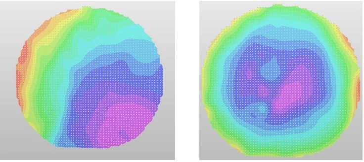
Comparison before and after the elimination of rigid-body displacement
2. Viewing Window Grid Distortion Correction Algorithm
In addition to inherent lens distortion, the glass viewing window of the high-low temperature chamber introduces extra refractive distortion that cannot be compensated for by conventional calibration. The system employs a grid-based correction algorithm to calculate the distortion field caused by the viewing window and apply inverse compensation, thereby ensuring measurement accuracy at every point across the entire wafer surface.
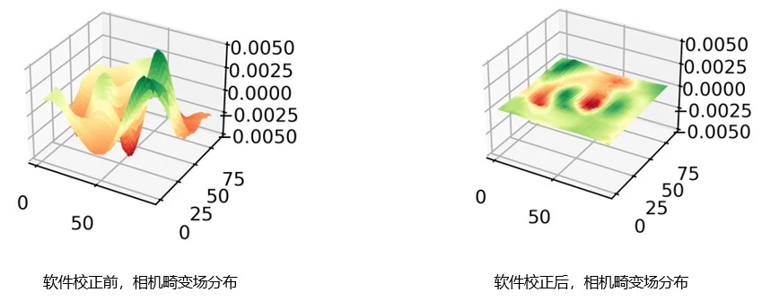
Comparison of window distortion before and after correction
V. Typical Case Study of Wafer Thermal Warpage Measurement Using DIC
5.1. Specimen Information
The specimen tested was a 6-inch single-crystal silicon wafer with a diameter of 150 mm and a thickness of 1 mm. Prior to testing, a high-temperature-resistant speckle pattern was applied to the wafer, and it was mounted in a thermal chamber using a free-boundary configuration.
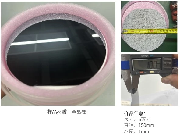
6-inch monocrystalline silicon wafer sample
5.2 Temperature Loading Procedure
The test temperature range spans 0°C to 150°C, with 10°C increments defining individual test conditions. Upon reaching the target temperature, the sample is held for 10 minutes before image acquisition is triggered. A total of 16 test stages (S₀–S₁₅) are conducted to fully document the evolution of wafer thermal warpage throughout the heating process. A 3D DIC strain measurement system simultaneously captures images, outputting 2D strain maps, 3D warpage topography, and average out-of-plane displacement data.
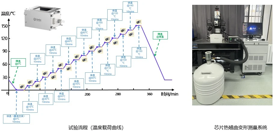
Temperature-Load Curve and DIC Testing System
5.3 Analysis of Test Results
The test results present 2D deformation maps and 3D warpage profiles of the wafer at various temperatures. As the temperature rises, the wafer's thermal warpage displacement continuously increases; at 120°C, the average displacement reaches 297 μm, marking the peak warpage deformation during the heating phase. With further temperature increases, the average warpage displacement exhibits a slight decrease due to the effect of material stress relaxation.
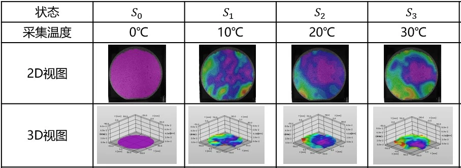
2D/3D thermal warpage results for temperature ranges S0–S3
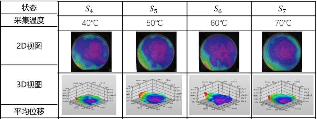
2D/3D thermal warpage results for the S4–S7 temperature range
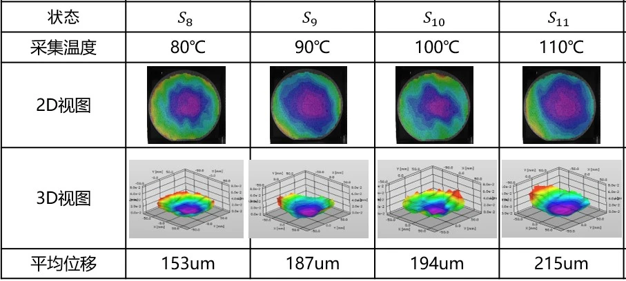
2D/3D thermal warpage results for temperature ranges S8–S11
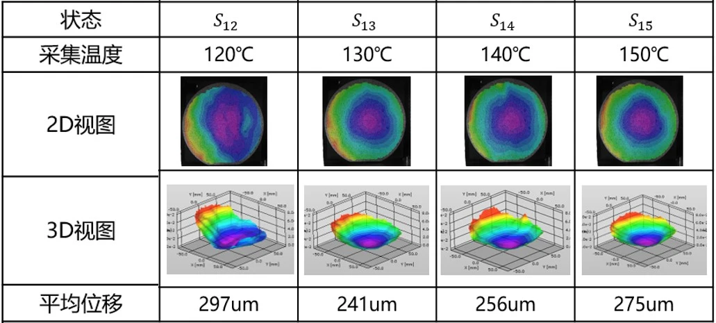
2D/3D thermal warpage results for the S12–S15 temperature range
The full-field data output by the DIC 3D strain measurement system allows for the intuitive visualization of varying degrees of wafer warpage across different regions and the identification of localized deformation concentrations. The obtained warpage magnitude and strain distribution data can be used to evaluate the thermal matching performance between the wafer and packaging materials, guide the optimization of packaging processes, and mitigate failure risks such as the "head-in-pillow" (HiP) effect, bridging, and open circuits.
VI. Application Value and Expansion Directions of the DIC Measurement System
Application Value
Digital Image Correlation (DIC)—specifically DIC 3D strain measurement—technology enables the inspection of thermal warpage, flatness, and coplanarity for wafers, substrates, BGAs, and IC packaging devices. It also facilitates the measurement of the Coefficient of Thermal Expansion (CTE) and full-field surface strain distribution of microelectronic materials.
Unlike single-point inspection methods, the DIC 3D strain measurement system fully captures the evolution of device deformation across the entire temperature profile. It quantifies thermal warpage amplitude, identifies localized deformation concentrations, and assesses the thermo-mechanical matching between different materials. This provides critical experimental data for the iteration of semiconductor packaging processes, material selection, and reliability verification, thereby reducing the risk of chip soldering failures at the source.
Expanded Testing Scenarios
1. Dynamic warpage testing of wafers and chip packages under simulated reflow soldering temperature profiles;
2. Thermal matching characteristic testing at the PCB-chip assembly level to evaluate the warpage compatibility between substrates and components;
3. High- and low-temperature cycling reliability testing for automotive chips and power devices;
4. Measurement of high-temperature deformation and the Coefficient of Thermal Expansion (CTE) for thin-film materials and MEMS devices.








 Video Center