Background
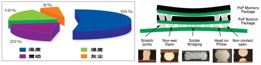
Research indicates that over 50% of semiconductor component failures stem from stress concentrations caused by heat generation. Differences in the coefficients of thermal expansion among various materials lead to stress concentrations during thermal cycling, causing semiconductor warping and subsequent failure. As semiconductor chip manufacturing technology advances, the stacking of vast numbers of transistors and complex packaging processes have made chips increasingly sensitive to temperature fluctuations. Consequently, thermal cycling testing has become an essential step during the chip design, packaging, and testing phases, creating an urgent need for a system capable of testing thermal deformation in semiconductor chips and performing high-precision measurement and analysis.
Distribution of Failure Factors in Semiconductor Components & Solder Joint Failures Caused by Chip Warpage
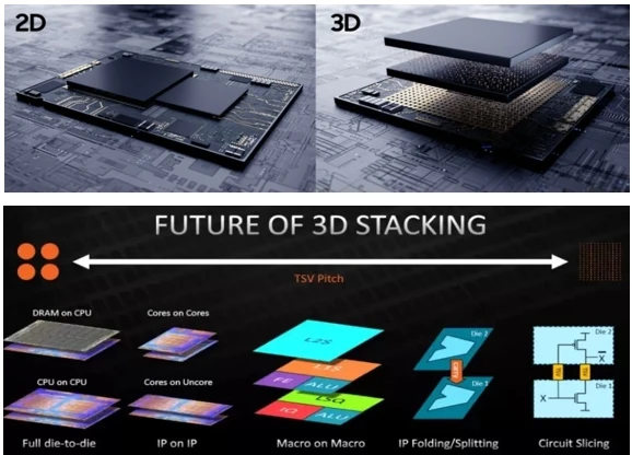
Chip warpage resulting from the trend toward high-density stacking presents greater challenges.
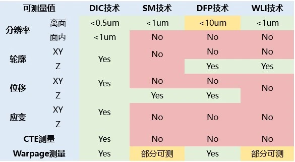
DIC Principles, Technology Comparison, and Significance
The XTOP3D XTDIC 3D full-field deformation measurement technology combines Digital Image Correlation (DIC) with binocular stereo vision. By tracking speckle patterns or feature patterns on an object's surface and performing stereo matching and 3D reconstruction, it enables the dynamic measurement of full-field 3D coordinates, displacements, and strains during deformation. Key features include non-contact operation, portability, high speed, high precision, ease of use, and real-time measurement capabilities. It is particularly well-suited for measuring chip thermal warpage and deformation.
Chip Warpage and Deformation Measurement Technology:
-
DIC technology(Digital Image Correlation)
-
SM technology(Shadow Morie)
-
DFP technology(Digital Fringe Projection)
-
WLI technology(White Light Interferometery)
The Importance of DIC Technology in Chip Failure Analysis:
By capturing contour data in a reference state, DIC technology enables the tracking of corresponding points as they undergo displacement under varying thermal loads, thereby allowing for the calculation and analysis of strain data.
Supported by this multidimensional data, chip failure analysis becomes both straightforward and reliable. It facilitates the simultaneous analysis of chip warpage and the evaluation of soldering processes, as well as the detection of strain concentrations across different materials in cross-sections; furthermore, measuring the Coefficient of Thermal Expansion (CTE) helps determine whether CTE mismatch issues are present.
System Components, Problems Addressed, and Key Metrics
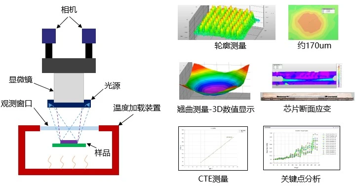
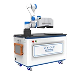
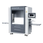
This solution utilizes the XTOP3D XTDIC-MICRO system. By integrating Digital Image Correlation (DIC), microscopy, and thermal stage technologies, the system is designed for scientific research and data analysis of semiconductor chips within a micro-scale field of view (1–10 mm).
A typical system for measuring chip thermal warpage comprises the following units:
-
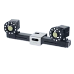
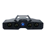
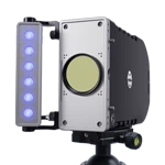
DIC measurement system: includes cameras, light sources, calibration plates and calibration fixtures, a speckle patterning kit, and software;
-
Microscope: Uses an optical microscope with approximately 10x magnification, equipped with two industrial cameras;
-
Temperature loading system: programmable temperature control supporting both heating and cooling;
This system enables in-depth analysis of the causes of chip failure, covering thermal warpage, 3D coordinates, 3D displacement and deformation, 3D strain distribution, and CTE measurement.
It supports the measurement of various semiconductor integrated circuits, including CPUs, GPUs, SSD chips, and SoCs. It facilitates reflow soldering process simulation, operational environment simulation, and analysis of various research and manufacturing processes.
Key specifications of XTOP DIC technology:
-
Non-contact measurement technology;
-
Full-field measurement of XYZ 3D coordinates, displacement, and strain;
-
Measurement field of view: 1–10 mm;
-
Maximum strain measurement accuracy: 20 µε;
-
Warping measurement accuracy: 0.1 µm;
-
CTE determination;
-
FEA comparison;
-
Maximum temperature range: -190°C to +600°C.
XTDIC-MICRO 3D Micro-scale Strain Measurement System Series: 1–10 mm measurement range
XTDIC-CONST 3D Full-field Strain Measurement System Series: Measurement range up to 500 mm
Key Technologies and Outcomes of the Solution
Measuring thermal deformation within the microscopic field of view presents numerous challenges.
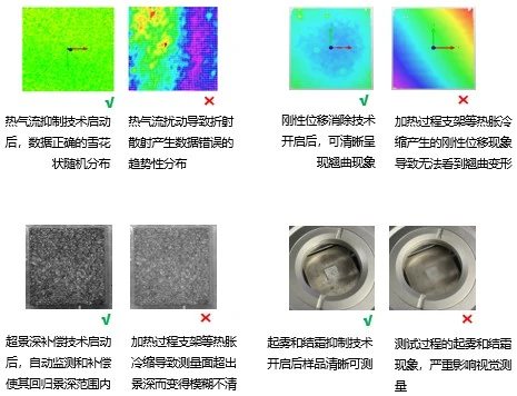
Leveraging years of accumulated technical expertise and project experience, XTOP has successfully overcome challenges that differ from those encountered in conventional DIC, ensuring a stable and reliable measurement process from start to finish.
-
Thermal airflow suppression technology
-
Rigid displacement elimination technology
-
Fogging and frosting suppression technology
-
Temperature compensation technology
-
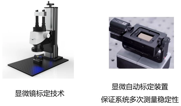
Microscopic automatic calibration technology
-
Extended depth-of-field compensation technology
Practical Case: Sample, Hardware System, and Test Procedure
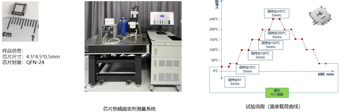
DIC Measurement Setup: This case demonstrates the measurement of thermal deformation in a chip (approximately 5 mm in size) subjected to a stepwise heating profile. Package Type: Quad Flat No-leads (QFN) Package.
Experimental Procedure: A cyclic test was designed, starting from room temperature (RT) and ramping up to 30°C. Data was recorded at 30°C, then at 50°C intervals from 100°C up to a maximum temperature of 245°C, followed by cooling back to room temperature at the same intervals. Data acquisition was performed after a 5-minute dwell period at each test point.
Case Study: Data and Analysis
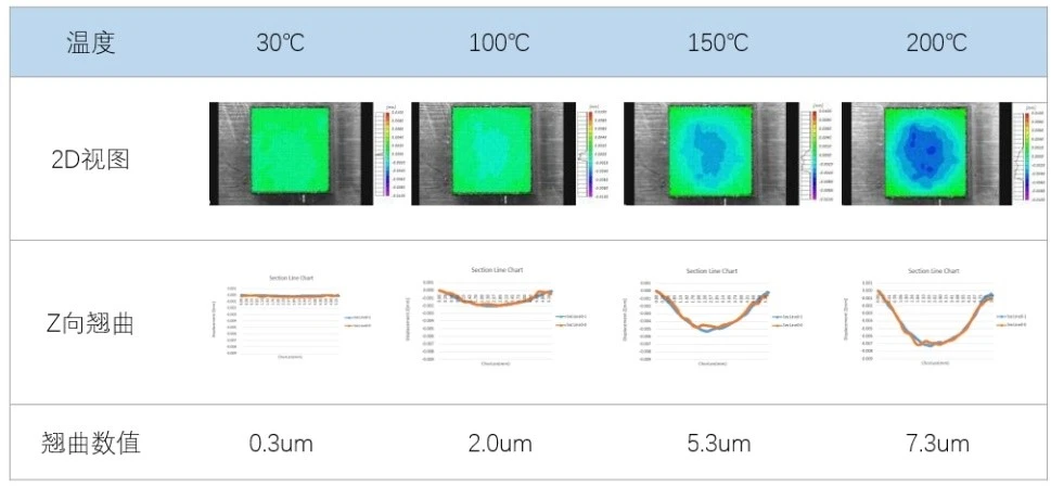
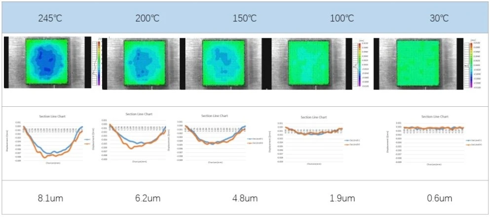
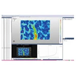
Measurement Data: The 2D warpage view, Z-axis warpage, and warpage values for the sample under a temperature cycle of 30°C – 245°C – 30°C are as follows:
Data Analysis
-
The chip exhibits symmetrical warpage at its four corners during thermal deformation, consistent with theoretical expectations;
-
The resolution of the initial static warpage is at the sub-micron level, and the accuracy meets the requirements;
-
Warpage increases with rising temperature, reaching a maximum of 8.1 μm at the peak temperature of 245°C;
-
Warpage gradually decreases as the temperature drops, returning essentially to the initial level upon cooling back to 30°C.









 Video Center