Semiconductor

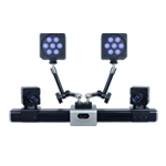
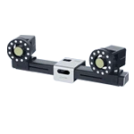
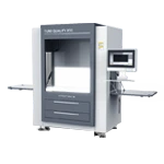
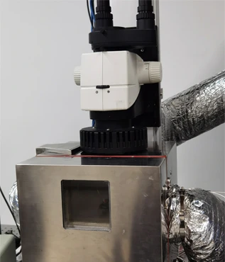
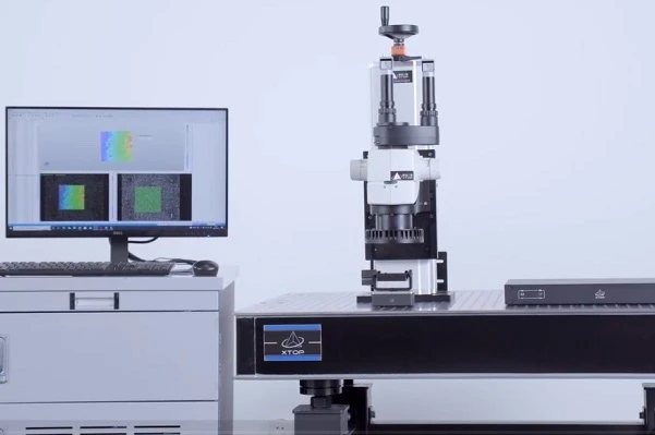
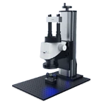
XTOP3D’s semiconductor thermal deformation and warpage measurement solution utilizes the high-precision XTDIC-MICRO 3D Microstrain system integrated with stereo microscopy. Designed for advanced chip packaging, PCBs, and single-crystal silicon, this non-contact DIC (Digital Image Correlation) technology provides real-time, full-field 3D strain and out-of-plane displacement analysis. It accurately evaluates CTE (Coefficient of Thermal Expansion) mismatch, solder joint reliability, and thermal warpage from micro-scale to full assemblies under varying temperature loads.

semiconductor warpage measurement, chip thermal warpage DIC, 3D microstrain measurement, microscopic DIC system, thermal deformation testing, Advanced Packaging warpage, PCB welding deformation, single crystal silicon CTE, coefficient of thermal expa
Video Center
Empowering Scenarios
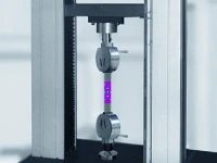
  • The XTDIC-MICRO micro-strain measurement system, when used with various in-situ loading testers, can perform multi-performance mechanical property tests such as tension, compression, and cycling on mesoscopic specimens, achieve full-field strain measurement of tiny specimens, and obtain stress-strain engineering curves.

    Mesoscopic material mechanical testing

    Mesoscopic material mechanical testing

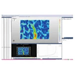
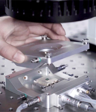
  • The XTDIC-MICRO microstrain measurement system, combined with an optical hot and cold stage, can analyze chip warpage at different temperatures, outputting warpage contours, curves, and strain data for each temperature point. It can also analyze the out-of-plane displacement of the chip surface to obtain the warpage distribution, and can analyze the full-field 2D displacement and strain fields.
    Chip thermal warpage test

    Chip thermal warpage test

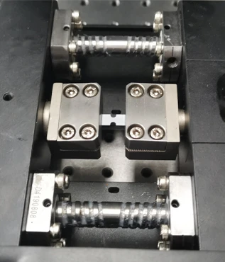
  • The XTDIC-MICRO microstrain measurement system, combined with an optical hot and cold stage for temperature loading, performs thermal expansion (CTE) tests on specimens, outputs CTE at different positions in the X and Y directions, and semiconductor thermal expansion test data, helping to improve the stability of semiconductor devices.

    Expansion coefficient test for circuit boards, single crystal silicon, etc.

    Expansion coefficient test for circuit boards, single crystal silicon, etc.

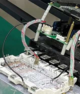
  • The XTDIC-MICRO microstrain measurement system, combined with a temperature-controlled chamber, analyzes the dynamic deformation of semiconductors during temperature changes and packaging process testing. This allows the mechanical properties of different chip cross-section materials to be evaluated under temperature changes, and the reliability of the materials can be verified by comparing them with the theoretical design values.

    Semiconductor deformation testing

    Semiconductor deformation testing

  • Application Cases
    • DIC Full-Field Measurement Solution for Chip Warpage and Thermal Deformation
      XTOP3D's full-field deformation measurement DIC technology acquires baseline profile data, tracks displacement data of identical points under varying temperature loads, and calculates and analyzes strain data. This allows for simultaneous analysis of chip warpage, soldering process evaluation, and strain concentration between different cross-section materials. CTE measurement can further identify chip thermal warpage and CTE mismatch issues.
    • Microscopic DIC technology for single crystal silicon thermal expansion warpage CTE measurement
      The thermal warpage experiment uses the Xintuo 3D XTDIC-MICRO microscopic strain measurement system and temperature controller (temperature control ±0.1°C). Based on microscopic DIC technology, a chip thermal warpage measurement platform is built to carry out thermal warpage tests on typical stacked structures, realizing real-time observation of thermal warpage of multilayer boards during heating.
    • DIC 3D Strain Measurement System Solution for Wafer Thermal Warpage and Deformation Measurement
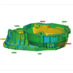
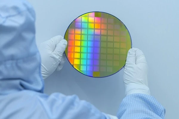
      During semiconductor manufacturing and chip packaging, thermal warpage in wafers is a critical factor leading to issues such as chip cracking, open solder joints, circuit shorts, device performance drift, and even total system failure. Leveraging the advantages of non-contact, full-field, and micron-level measurement, Digital Image Correlation (DIC) technology—specifically 3D strain measurement systems—can capture comprehensive data on 3D warpage morphology, displacement fields, and strain fields across the entire temperature range. This provides a quantitative basis for optimizing wafer processes, designing for thermal matching in packaging, and validating the reliability of automotive-grade chips.

    • Contact Us
      Contact Us

      Welcome for business negotiations. We look forward to cooperating with you.

    • 3D microscopic DIC system, microscopic strain measurement, microscale deformation analysis, XTDIC-MICRO, XTOP3D, digital image correlation microscope, chip thermal warpage measurement, semiconductor CTE testing, micro-material mechanical testing, full-field strain measurement, micro-DIC system, 3D microstrain measurement, microscale in-situ loading, CTE parameter determination, electronic packaging reliability test, advanced packaging warpage DIC, microscale displacement tracking
      Featured Products

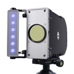
      3D microstrain measurement system