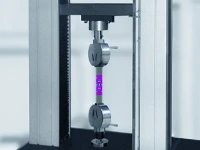
Wafer thermal deformation testing is a critical aspect of semiconductor manufacturing and materials research. Failure to adequately account for differences in the coefficients of thermal expansion among chip materials can lead to wafer warpage or cracking, resulting in circuit short circuits, performance drift, or even device failure. Consequently, predicting thermal deformation trends in advance has become a fundamental requirement for effective chip design.
Applications involving wafer thermal deformation span a wide range of areas, including high-temperature wafer deposition and etching processes in semiconductor manufacturing and packaging; performance testing of consumer electronics (3C devices) in extreme environments; data measurement for AEC-Q100 certification of automotive chips; and risk assessment of thermal deformation during the long-term high-temperature operation of 5G base station components and high-performance computing chips. Accurately capturing thermal deformation data and trends yields significant benefits and has a profound impact on industries associated with wafers and chips.
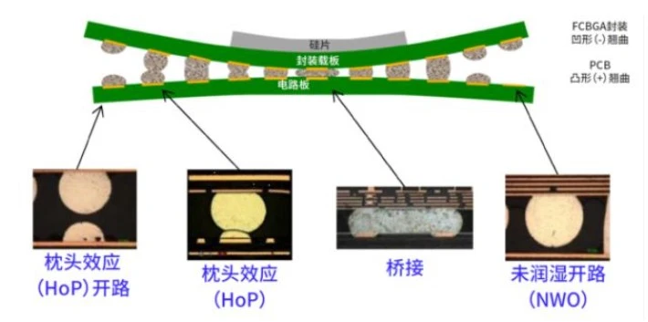
Solder joint failure caused by chip warpage
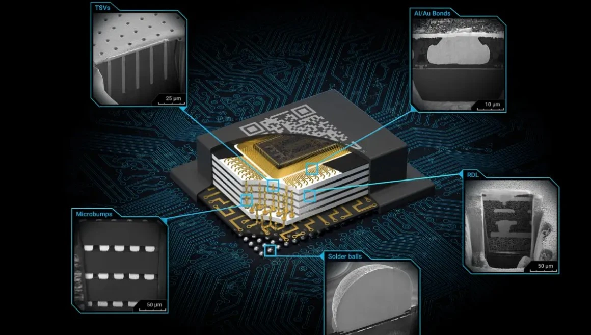
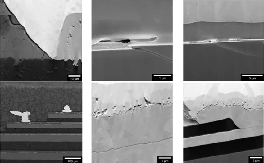
Improper analysis of thermal deformation leads to various failure phenomena.
Advantages of DIC Technology
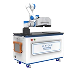
The XTOP3D XTDIC 3D full-field strain measurement and analysis system is based on Digital Image Correlation (DIC) technology. By integrating binocular stereo vision and close-range photogrammetry, it tracks speckle patterns on the object's surface to measure 3D coordinates, displacement, and strain during deformation.
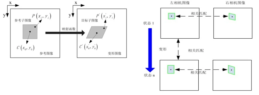
Schematic diagram of the principles of Digital Image Correlation (DIC) technology
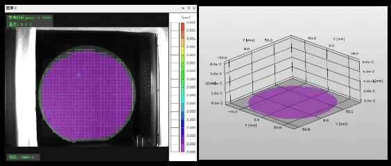
Schematic diagram of wafer thermal deformation measurement and analysis
Comparative Analysis of Wafer Thermal Deformation Measurement Techniques
-
DIC technology(Digital Image Correlation)
-
WLI Technology(White Light Interferometery)
-
Strain gauge(resistance strain gage technique)
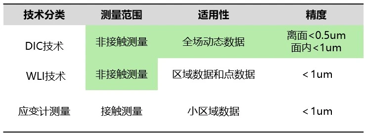
Advantages of DIC Technology
The advantages of DIC technology in wafer thermal strain measurement include high resolution (sub-pixel level), non-contact measurement (preventing damage), full-field analysis (capturing strain distribution across the entire surface), rapid data acquisition (real-time analysis), high adaptability (adjustable equipment and conditions), versatility (suitable for both static and dynamic monitoring), and data visualization (intuitive display of strain fields). These characteristics make it widely applicable in the semiconductor industry, helping to enhance product quality and reliability.
Application of DIC Technology in Wafer Thermal Deformation Measurement
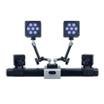
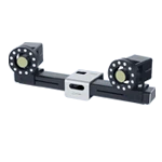
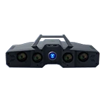
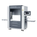
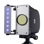
The wafer thermal strain measurement system is based on the principle of Digital Image Correlation (DIC). Its core components consist of the XTDIC-CONST 3D full-field strain measurement sensor head and a high/low-temperature test chamber. The system is designed for various temperature-dependent experiments and supports the measurement of data such as strain fields and displacement fields.
The main components of the XTDIC-CONST 3D full-field strain measurement system are as follows:
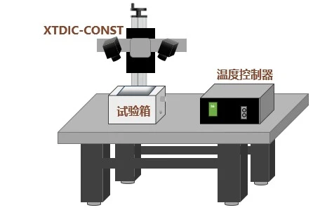
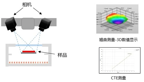
In the wafer thermal deformation measurement setup, the specimen is placed inside a sealed test chamber. A temperature controller monitors the internal temperature and regulates it by coordinating heating and cooling modules.
During the test, the XTDIC-CONST 3D full-field strain measurement system acquires data through a glass viewing window at the top of the chamber. Throughout the process, the temperature controller transmits real-time temperature data to the XTDIC software; the software uses this real-time data to manage the temperature sensors and trigger data acquisition at specific temperature points, thereby enabling automated control.
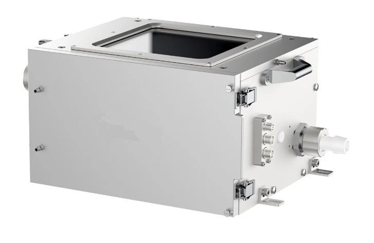
High and Low Temperature Test Chamber – Temperature Range: -40°C to 200°C
Measuring thermal strain in wafers using DIC (Digital Image Correlation) technology presents a series of challenges. Drawing on years of accumulated technical expertise and project experience, XTOP has successfully overcome challenges that differ from those encountered in conventional DIC applications, ensuring a stable and reliable measurement process.
1. Rigid-body displacement
During testing, temperature fluctuations—whether rising or falling—affect not only the test specimen but also other components within the chamber and the chamber's support structure. As these elements undergo thermal expansion, the test specimen experiences rigid-body displacement, which can impact the actual data. To address this, a rigid-body displacement elimination technology has been developed; when activated, it filters out displacement caused by external environmental factors, ensuring that only the specimen's intrinsic changes are displayed.
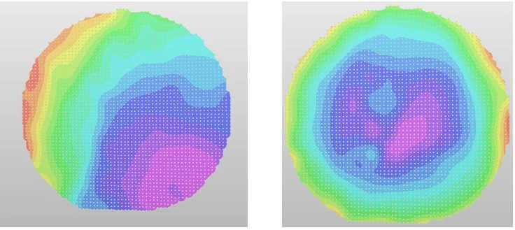
Before rigid-body displacement removal (trend influenced by external factors) / After rigid-body displacement removal (showing only the intrinsic trend)
2. Distortion Correction
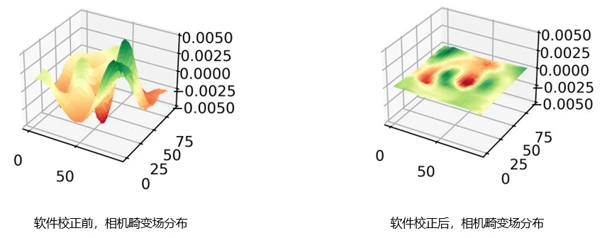
The wafer thermal strain measurement system involves not only lens distortion but also distortion caused by the top viewing window of the high-low temperature chamber; consequently, conventional calibration methods—which address only lens distortion—struggle to mitigate the interference introduced by the external glass. The software supports a grid-based correction algorithm that calculates the degree of grid distortion within the field of view and applies inverse compensation, thereby significantly reducing data errors across the entire field.
Representative Case Study
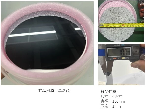
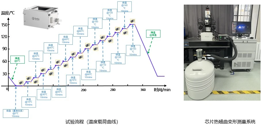
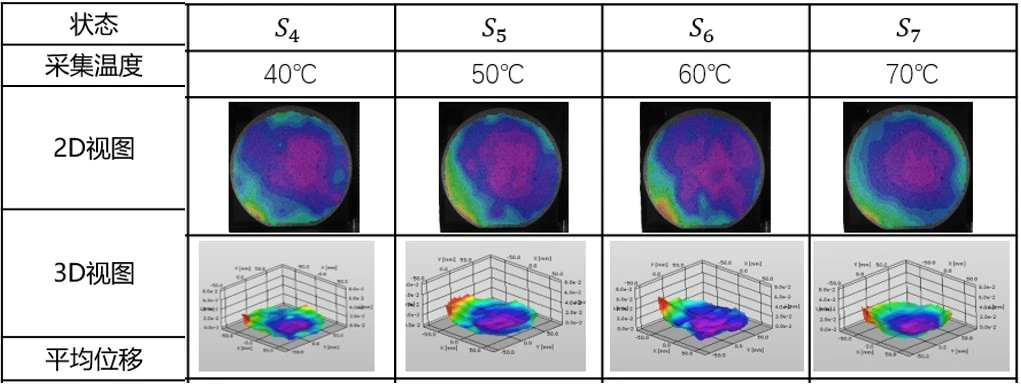
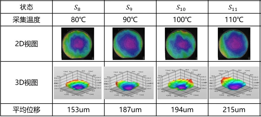
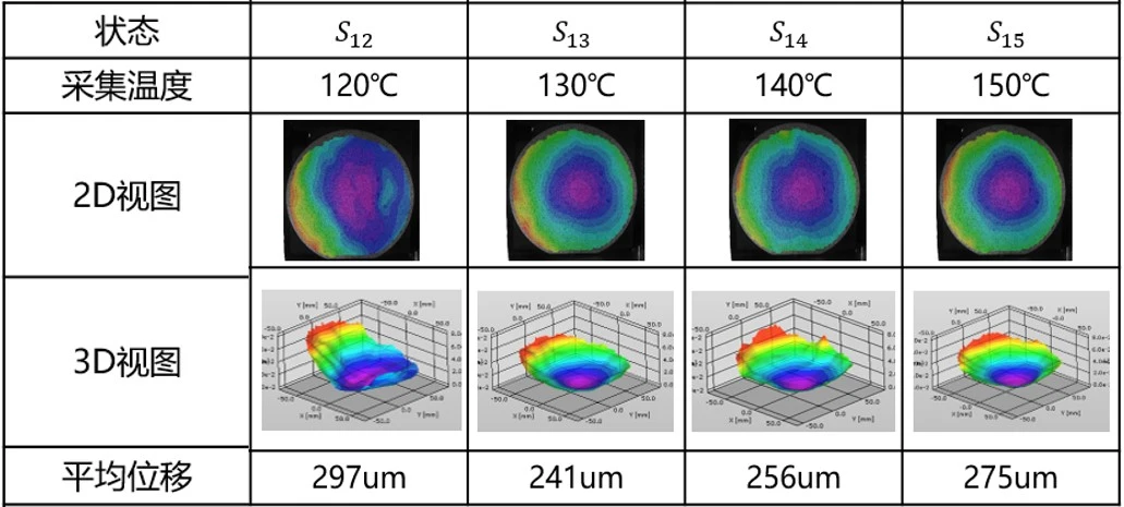
The wafer thermal strain measurement protocol is outlined below. The experiment is structured into test stages (designated S_x) at 10°C intervals (comprising 16 stages in total, labeled 0 through 15, as shown in the figure). Upon reaching each target temperature, the environmental chamber automatically maintains the temperature for 10 minutes before image acquisition takes place. The experiment spans a temperature range from 0°C to 150°C; the detailed calculation steps are presented in the table below:
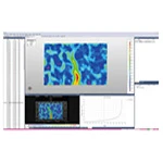
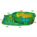
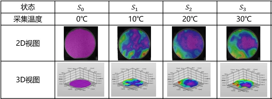
The results of the wafer thermal strain measurements are shown in the figure below. The status bar corresponds to the respective test stages in the chart, and the data is displayed using both 2D and 3D views, allowing for a clear visualization of the wafer's thermal strain distribution and deformation trends. Detailed test results are presented in the table below:
By integrating DIC technology with a high-low temperature test chamber, a thermal deformation and warpage measurement system is created. This system enables the assessment of thermal matching characteristics between printed circuit boards (substrates) and components across varying temperature ranges, allowing for the inspection of warpage in substrates and components under conditions that simulate the temperature fluctuations of reflow soldering.
By measuring changes in sample warpage and analyzing the matching characteristics between substrates and components, the system helps ensure product soldering quality and reliability.
XTOP3D DIC equipment is suitable for measuring the flatness and coplanarity of microelectronic devices—such as PCBs, substrates, BGAs, ICs, packaged wafers, and film-frame wafers—under thermal deformation conditions. It can also be used to measure the coefficient of thermal expansion (CTE) and surface strain distribution of microelectronic materials.