As electronic products evolve toward thinner, smaller, and higher-density designs, traditional rigid PCBs often fail to meet specific structural and performance requirements. Flexible PCBs (FPCs)—capable of bending, folding, and stretching—are widely used in mobile phones, cameras, wearable devices, medical electronics, and automotive electronics. Since an FPC's performance can change significantly after bending, bending tests are conducted prior to shipment to determine the circuit's tolerable bending radius and ensure the board's long-term reliability and consistency.
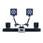
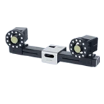
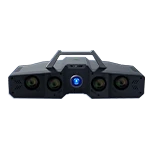
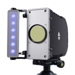
The XTOP3D XTDIC 3D full-field strain measurement system utilizes non-contact Digital Image Correlation (DIC) technology. By employing high-resolution industrial cameras and image processing, the system captures full-field displacement and strain distributions on the specimen's surface. It extracts data on shape, deformation, displacement, and strain, effectively visualizing the deformation process. This enables researchers to gain an intuitive and quantifiable understanding of material behavior across various conditions—from material-level to structural-level analysis and from ambient to high temperatures.

The XTOP3D XTDIC 3D full-field strain measurement system supports scientific research and engineering applications with specialized functional modules covering the entire workflow—from initial camera calibration and speckle pattern optimization to 3D coordinate reconstruction, displacement field calculation, and strain field analysis. It generates comprehensive result visualizations, such as full-field strain maps, displacement vector fields, and principal strain directions, while also supporting direct comparison with finite element analysis (FEA) results.
In industrial applications, the XTDIC system is particularly well-suited for:
· Characterization of material mechanical properties (e.g., elastic modulus, Poisson's ratio)
· Structural strength verification (fatigue, crack propagation analysis, weld deformation measurement)
· Study of composite material anisotropy
· Material behavior testing in high-temperature environments
· Vibration and mode shape analysis
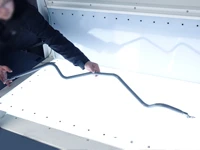
Bending Measurement of Flexible Circuit Boards
The core advantage of the XTDIC 3D full-field strain measurement system lies in its ability to perform high-precision full-field displacement and strain analysis, achieving sub-pixel displacement resolution (at the 0.01-pixel level) and a strain measurement accuracy of 20 με.
Its non-contact nature makes it particularly suitable for testing scenarios—such as flexible materials and high-temperature components—that are challenging for traditional sensors. Furthermore, the intuitive output of strain maps and displacement vector fields provides direct data support for simulation validation (e.g., FEM comparison).

Experimental Setup
Equipment: XTDIC 3D full-field strain measurement system (5 MP resolution, >500 fps, measurement area: 64 × 48 mm); speckle pattern preparation (application of matte black and white spray paint).
Specimen: Flexible circuit board.
Procedure:
Secure the specimen in the fixture and capture a reference image in the initial state;
Manually apply external force: use a finger to bend the specimen toward the DIC camera to a specific curvature;
Slowly release the external force: allow the specimen to naturally return to its initial planar state;
The DIC system continuously records the image sequence of the flexible circuit board's surface throughout the process.

Data Analysis
Due to the presence of components, lattice structures, and surface irregularities (such as protrusions and indentations) on the specimen, the analysis focuses on planar deformation data within key regions. DIC software is used to analyze the evolution of the strain field in the flexible circuit board during bending, providing quantitative data to support structural optimization and failure prediction.
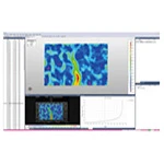
Reconstruction of Full-Field Displacement and Strain Fields
3D coordinate reconstruction: DIC dual-camera image matching generates 50 sets of 3D point cloud data per second for the material surface;
Calculation of key parameters:
Full-field displacement vector field (displacement contour maps in X, Y, and Z directions)
Maximum principal strain field (representing the maximum strain in the material's bending direction)
1. Displacement field data for critical regions of the specimen
Displacement field: Reveals the bending deformation mechanism.


Seven key functional points on the specimen surface (such as chip pads and wire bend points) were selected to analyze the resultant surface displacement data under bending stress, as well as the specimen's recovery to its initial state after the bending force was released.
Displacement curves for the seven key functional points:

2. Strain field data for critical regions of the specimen
Strain field: Locating regions sensitive to failure
The maximum shear strain field identifies the critical zone for bending deformation.


Seven critical functional points on the specimen surface (such as chip pads and conductor bend points) were selected to analyze the strain evolution during the bending process and the maximum principal surface strain data, as well as to assess the risk of material plasticity revealed by irreversible deformation.
Strain curves for the seven critical functional points:

Summary of Test Data
Using the XTOP3D XTDIC 3D full-field strain measurement system, the deformation of flexible materials under bending loads can be accurately and effectively monitored. The system captures localized strain concentrations that are undetectable by traditional methods and analyzes full-field displacement and strain. The comprehensive data is fully traceable, allowing for comparative analysis against finite element results and serving as a digital record for product reliability verification.


The XTOP3D XTDIC 3D full-field strain measurement system enables high-precision, full-field deformation measurement. It provides visualized full-field data that intuitively highlights areas of concentrated deformation—such as crack initiation sites—thereby helping researchers rapidly pinpoint issues. By applying DIC technology, the system successfully quantifies the 3D strain distribution of flexible circuit boards during bending and recovery cycles; it reveals strain gradient patterns through multi-feature-point analysis and facilitates "test-simulation" closed-loop optimization via FEA comparison. This methodology provides high-precision data to support the evaluation of bending performance and material deformability in flexible electronic devices.