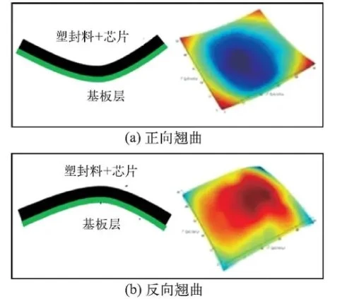
Die warpage has become an increasingly significant concern in advanced packaging; differences in the coefficients of thermal expansion (CTE) among the various materials within the die lead to thermal deformation mismatches, thereby generating mechanical stress and warpage. In the field of microelectronic packaging, thermal warpage is a common phenomenon throughout the stages of component manufacturing and service; for instance, die fabrication processes themselves can induce thermal warpage. Furthermore, self-heating during operation and fluctuations in ambient temperature can also cause component warpage and deformation. Excessive warpage can lead to issues such as die cracking, die delamination, and solder joint failure.
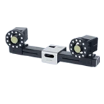
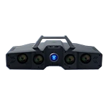
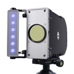
In the experimental observation of structural thermal warpage, the primary focus is measuring out-of-plane displacement caused by the warpage. The XTOP3D XTDIC-MICRO 3D microscopic strain measurement system—which integrates Digital Image Correlation (DIC) technology with a stereo microscope—can be used to measure surface deformation, strain, and warpage in chip specimens subjected to applied loads and varying temperatures. By utilizing the stereo microscope alongside software designed for complex distortion correction, high-magnification measurements can be achieved, making the system suitable for measuring Z-axis displacement and warpage in chips.
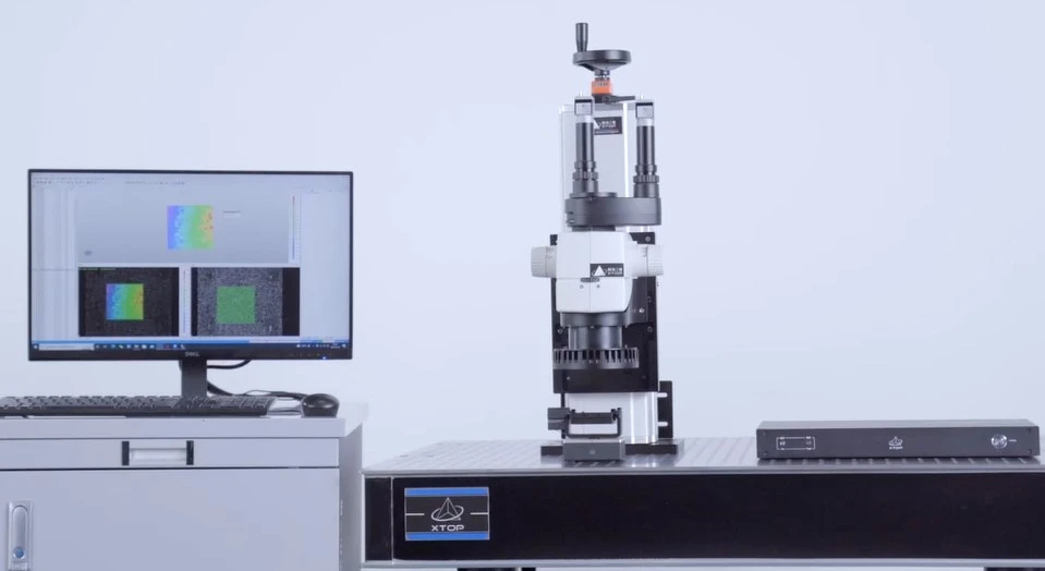
The XTDIC-MICRO 3D microscopic strain measurement system features a one-click automatic calibration function that corrects image distortion, thereby avoiding issues associated with traditional parametric distortion models. By calculating the non-parametric distortion field of the stereo microscope, this calibration method completely eliminates topography and strain measurement errors.
Limitations of Traditional Measurement Methods
-
Contact-based measurement methods primarily include the shim method and the contact probe method; while the former is low-cost and simple to operate, it offers relatively low measurement accuracy.
-
Although the contact probe method offers high accuracy, it cannot achieve full-field measurement or dynamically monitor deformation and warpage resulting from temperature changes.
-
Regarding non-contact methods, the Moiré fringe technique requires close proximity to the sample surface, imposing significant limitations on measurements in high-temperature environments.
-
Interferometry offers high measurement accuracy but is unsuitable for high-temperature applications due to the close proximity required between the lens and the sample; additionally, it suffers from drawbacks such as a limited field of view, long measurement times, and complex, expensive optical setups.
Micro-DIC Solution for Thermal Warpage Measurement
Measuring chip warpage places high demands on the proximity between the sample and the lens; conducting measurements in high-temperature environments carries a risk of damaging the lens due to heat. The XTDIC-MICRO 3D microscopic strain measurement system from Xintuo 3D overcomes these limitations through high-speed, non-contact measurement, making it ideal for the real-time observation of thermal warpage processes.
To effectively monitor thermal warpage, a measurement platform based on micro-DIC technology was established. Thermal warpage tests were conducted on typical stacked structures, enabling real-time observation of the warpage occurring in multi-layer boards during heating.
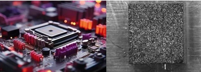
Fabricating high-temperature-resistant speckle patterns on the chip surface.
Chip heating tests at various temperatures
The thermal warpage experiment utilized the XTDIC-MICRO microscopic strain measurement system from Xintuo 3D, along with a temperature controller (precision ±0.1°C) and a cooling controller. The optical thermal stage was equipped with a thermal insulation cover and an observation window to minimize sample disturbances caused by airflow.
During the experiment, an appropriate heating stage temperature control program was established based on the furnace temperature profile, and the test temperatures were categorized into three groups:
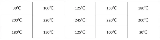
Note: The operating temperature and self-heating temperature of standard chips generally do not exceed 200°C; 150°C is also a common benchmark for thermal testing specified in the standard *GJB 548B-2005: Test Methods and Procedures for Microelectronic Devices*.
The XTDIC-MICRO microscopic strain measurement system captures images throughout the entire warpage process; the Region of Interest (ROI) is defined as the sample's entire top surface, and the DIC software is used for 3D model reconstruction and post-processing of relevant parameters.
Experimental data on chip warpage during heating
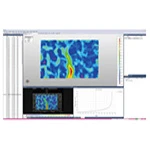
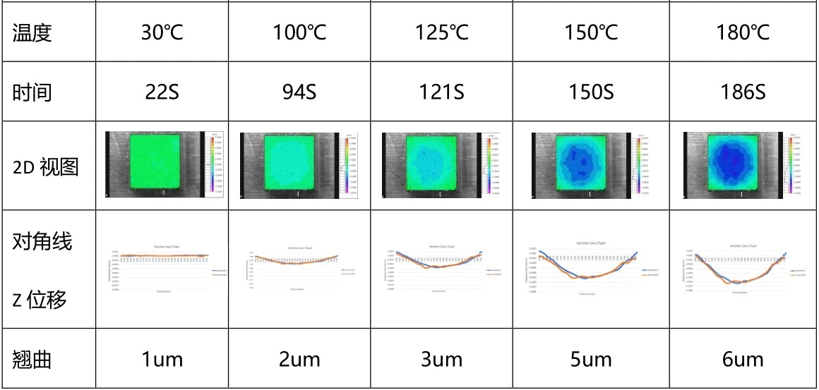
DIC software is used to analyze and calculate the chip's warpage at various temperatures, generating warpage contour maps, graphs, and strain data for each temperature point.
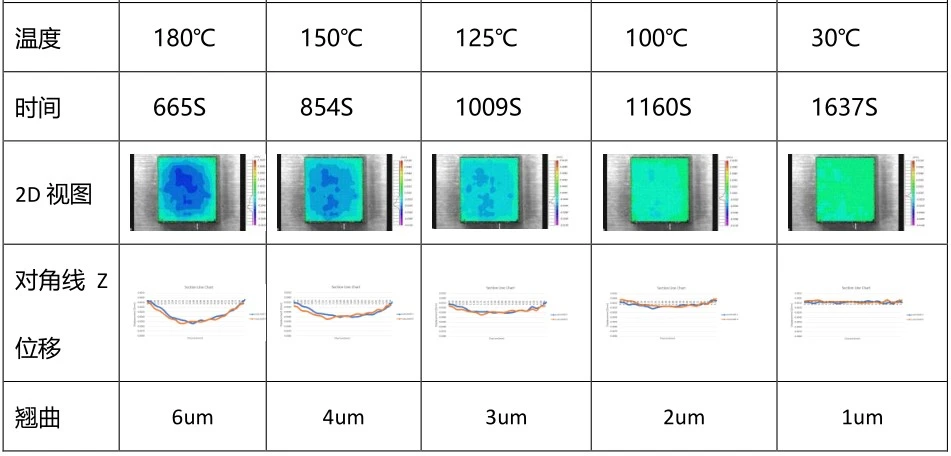
The figure below shows the warpage distribution derived from analyzing the out-of-plane displacement of the chip surface as it is heated from 30°C to 180°C. The system enables analysis of full-field 2D displacement and strain fields as well as diagonal Z-axis displacement variations; the measured maximum warpage is 6 µm.
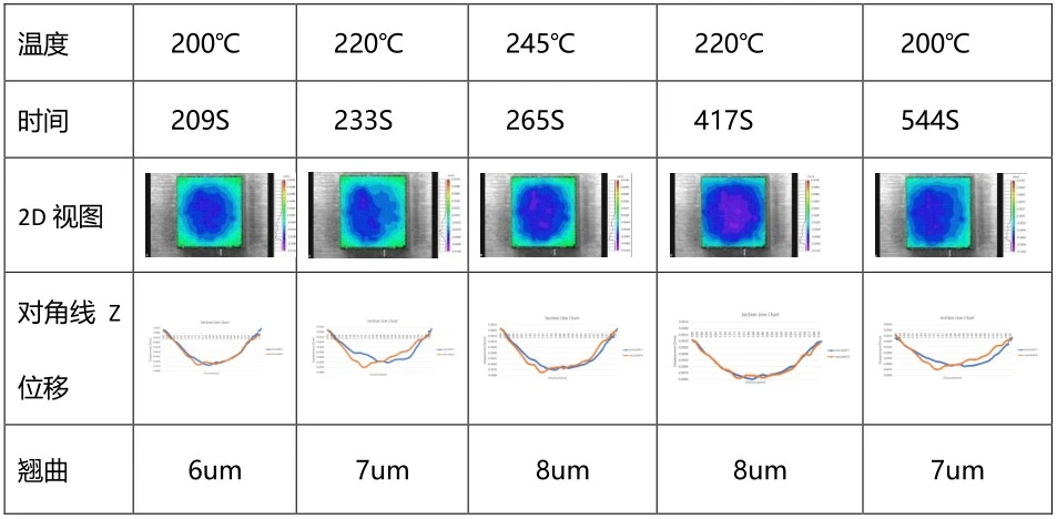
The figure below shows the warpage distribution obtained by analyzing the out-of-plane displacement on the chip surface as the chip is heated from 200°C to 245°C and then cooled back to 200°C. This allows for the analysis of full-field 2D displacement and strain fields, as well as Z-axis displacement variations along the diagonal; the maximum measured warpage is 8 µm.
The figure below shows the warpage distribution obtained by analyzing the out-of-plane displacement on the chip surface as the temperature drops from 180°C to 30°C; this allows for the analysis of full-field 2D displacement and strain fields, as well as diagonal Z-axis displacement variations, with a measured maximum warpage of 6 μm.
The XTOP3D XTDIC-Micro series microscopic strain measurement system integrates a binocular stereo microscope to enable mechanical behavior testing within millimeter-scale fields of view. It facilitates the measurement of 3D coordinates, displacement, and strain on the surfaces of micro-scale objects across varying temperatures. Suitable for CTE measurements of ICs, chips, semiconductors, and electronic components, the system plays a crucial role in testing the mechanical properties related to thermal warpage during chip manufacturing and packaging processes.