Background of DIC Testing
Thermal deformation and warpage of monocrystalline silicon are common phenomena during high-temperature processing of integrated circuits and other silicon-based devices, representing one of the most critical and challenging issues in device fabrication. Silicon wafer warpage complicates the photolithography process for complex circuit patterns, significantly impacting device yield and performance.
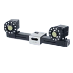
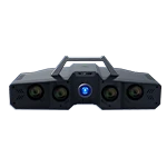
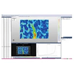
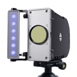
By utilizing the XTOP3D XTDIC 3D full-field strain measurement system in conjunction with a temperature control chamber, thermal deformation testing of monocrystalline silicon in high-temperature environments can be conducted. The DIC technique tracks speckle patterns on the material's surface to calculate displacement field distributions across various deformation states, enabling the analysis of thermal deformation and warpage characteristics.
DIC Test Specimen
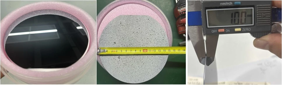
The single-crystal silicon specimen measures 6 inches (150 mm in diameter and 1 mm in thickness).
DIC Test Objective
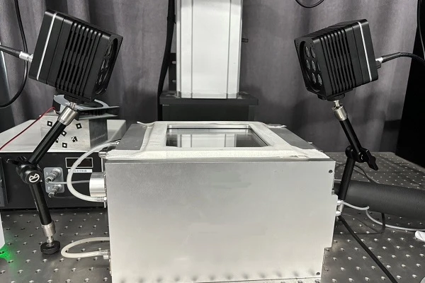
A monocrystalline silicon specimen is heated within a temperature-controlled chamber. The XTDIC 3D full-field strain measurement system is used to measure the full-field displacement distribution, providing the client with data on full-field displacement and deformation.
Thermal Deformation Test Method
The monocrystalline silicon specimen is heated from 0°C to 150°C at a rate of 5°C/min within the temperature-controlled chamber. Data is captured and analyzed at 10°C intervals to examine the displacement field distribution of the specimen at various temperature stages.
Given the large dimensions of the monocrystalline silicon specimen—compared to tests involving microscopic analysis or low-resolution lenses—the accuracy of the DIC analysis may be influenced by the field of view; therefore, it is necessary to verify the uniformity of the static data distribution.
To validate the accuracy of the XTDIC system, static accuracy verification is performed. Additionally, comparative analysis of deformation data is conducted—accounting for stress relief at high temperatures and potential interference from internal/external circulation fans—to ensure and enhance the feasibility and accuracy of testing in high-temperature environments.
DIC Test Accuracy Verification Strategy
1. DIC Static Accuracy Verification
The XTDIC 3D full-field strain measurement system is positioned for testing. During verification, parameters such as the light source, camera angles, camera separation, and measurement distance are adjusted in real-time (to ensure that the captured data is not compromised by the inherent precision limitations of the equipment itself).
Static Accuracy Verification Data
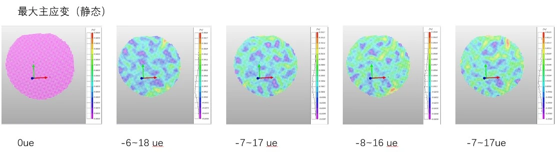
Five static images are captured using the XTDIC 3D full-field strain measurement system at the optimal testing position to analyze the maximum principal strain of the monocrystalline silicon specimen. Measured data indicates a maximum principal strain of no more than 20 με, demonstrating that the DIC testing accuracy has reached the desired level.
2. High-Temperature Stress Relief
Place the specimen in the environmental chamber and raise the temperature to 200°C. Maintain this temperature for at least 30 minutes to relieve the material's internal stresses, then allow it to cool naturally to room temperature. (This prevents internal material stresses from interfering with the data.)
3. Internal Circulation Fan Interference
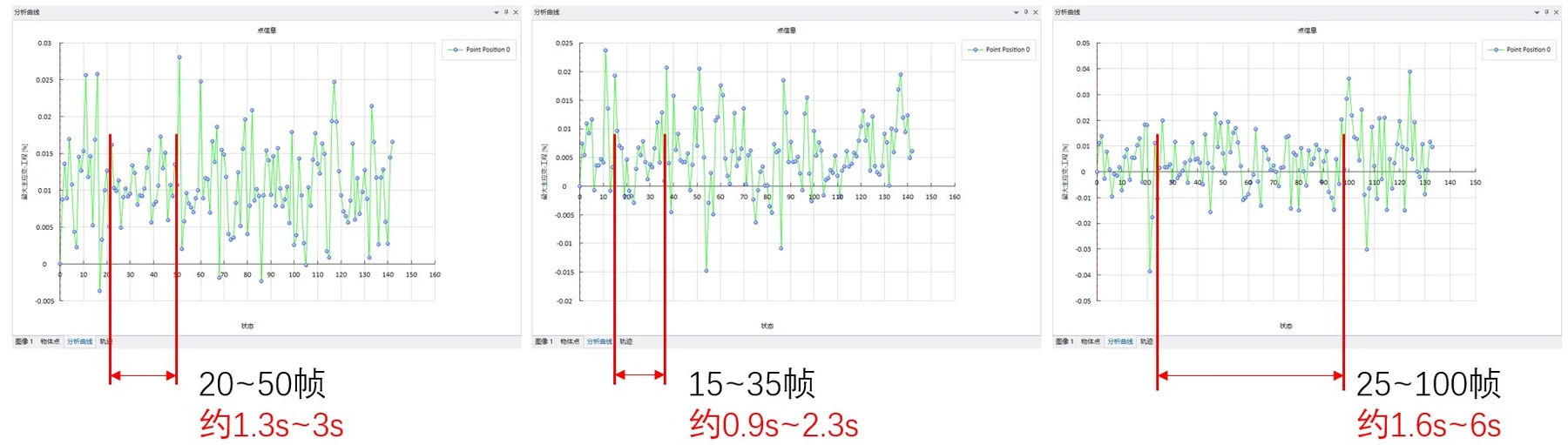
Since the internal circulation fan is rigidly connected to the environmental chamber, the chamber is subject to vibration interference from the fan. The period during which the data remains most stable after the fan is turned off is identified and selected as the DIC image acquisition window. (This eliminates interference from the internal fan and high-temperature airflow.)
Internal Circulation Fan Disturbance Test Data
Image acquisition using the XTDIC 3D full-field strain measurement system is initiated simultaneously with the switching off of the internal circulation fan; three sets of data are collected, each lasting approximately 20 seconds. The stability of the resulting curves is then analyzed. Measurements indicate that the data distribution is most uniform and fluctuations are minimal during the interval of 1.2 to 2.5 seconds after the fan is turned off.
4. External Fan Interference
During the heating process of the environmental chamber, thermal air currents form near the top glass viewing window; an external fan blowing horizontally is required to disperse these currents. (Assessing the impact of the external fan on the data)
External Fan Interference Test Data
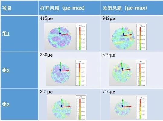
The sample was heated to 100°C and held at that temperature for 30 minutes. Data was then acquired using the XTDIC system with the external fan turned on, followed by a separate acquisition with the fan turned off. Three sets of data were collected with 5-minute intervals between them to analyze the effect of the fan's operation on the measurement results. Five images were captured during each acquisition, and the maximum strain value from each set was analyzed. (Theoretically, the calculated strain values derived from multiple images should be as low as possible.)
Measured data indicate that the data obtained with the fan turned on were significantly more stable and exhibited minimal fluctuation.
DIC Test Results
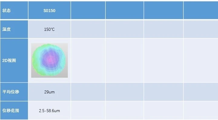
Using the XTOP3D XTDIC 3D full-field strain measurement system, the displacement field on the surface of the monocrystalline silicon specimen during heating was obtained; the table below clearly shows the deformation of the monocrystalline silicon material under thermal loading.
The DIC software features a built-in thermal expansion (CTE) function, which was used to analyze the CTE distribution of the monocrystalline silicon specimen. Shown below is the displacement field distribution of the specimen during the heating process:
Table 1
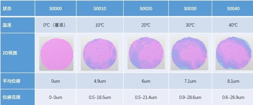
Table 2
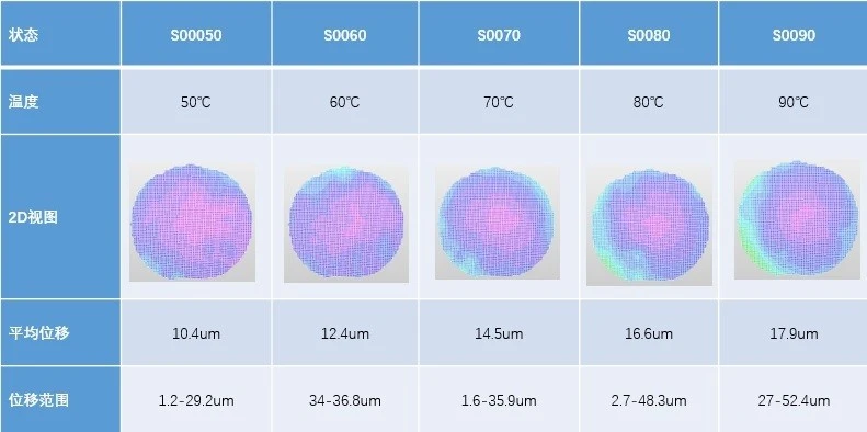
Table 3
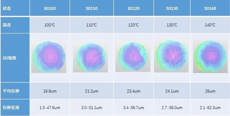
Table 4
Display of Basic Status Data
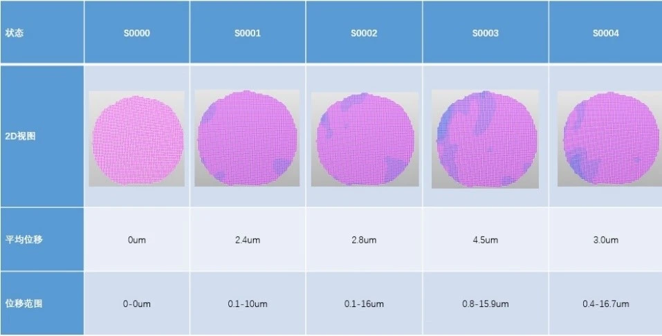
Basic status data serves as an indicator for monitoring fluctuations in the DIC camera's baseline frame data; these fluctuations reflect the degree of data variation during the overall equipment acquisition process.
Table 5
The XTOP3D XTDIC 3D full-field strain measurement system was employed in conjunction with a temperature-controlled chamber for thermal loading to conduct non-contact deformation testing in a high-temperature environment. This setup—integrating DIC technology with a temperature-controlled chamber to apply thermal loads ranging from room temperature to 200°C, and utilizing internal and external circulation fans to eliminate interference from hot air currents—offers advantages such as precise temperature control and accurate, reliable DIC displacement measurements.
Test Conclusions
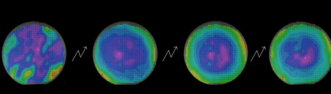
The XTDIC 3D full-field strain measurement system enabled the analysis of displacement fields on the surface of monocrystalline silicon specimens across various temperature environments. Test data reveal that as the temperature rises, the displacement field exhibits a trend of increasing magnitude from the center toward the edges—characterized by lower displacement at the center and higher displacement at the periphery. The data on thermal deformation of the monocrystalline silicon surface provide validation for material and structural simulation analyses, which is of significant importance for enhancing the manufacturing quality and reliability of semiconductor devices.