As electronic products evolve towards miniaturization, high density, and high performance, chips experience significant thermal deformation and warping during operation. This deformation not only affects package reliability but can also lead to serious problems such as solder joint failure and circuit breaks.
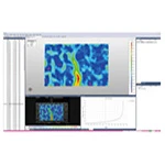
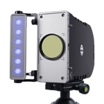
The micro-DIC strain measurement system can monitor the deformation behavior of chips in real time at a microscale during temperature changes, providing accurate data support for thermal design and reliability assessment.
I. Causes of Chip Thermal Deformation and Warpage
Mismatch in coefficients of thermal expansion: Differences in CTE among chip, substrate, and packaging materials lead to thermal stress concentration.
Increased power density: High-performance chips generate a lot of heat and their temperature rises rapidly.
Complexity of multi-layered structures: Different material layers deform inconsistently during thermal cycling.
Residual stress from manufacturing processes: initial stress generated during welding and packaging.
II. Advantages of Micro-DIC in Chip Thermal Deformation Measurement
Non-contact full-field measurement: does not interfere with the chip's operating state and avoids additional stress.
High spatial resolution: It can distinguish micron-level warping and local deformation.
Real-time dynamic monitoring: Captures the deformation evolution throughout the entire heating and cooling process.
Multi-region synchronous analysis: Simultaneously measure the strain distribution in multiple key regions on the chip surface.
III. Experimental Methods and Procedures
Sample preparation: speckle patterns are prepared on the chip surface to ensure stability at high temperatures.
Temperature control platform setup: A high-precision temperature control station is used to achieve stable heating and cooling.
Image acquisition: Images of the chip surface are captured at different temperature points.
Data processing: The displacement and strain fields were calculated using DIC software to analyze the warping morphology.
Results verification: The accuracy of the measurement was verified by comparing the results with those of the finite element thermal stress simulation.
IV. Typical Application Cases
1. Chip package warpage assessment
Under the reflow soldering temperature profile, the micro-DIC can record the chip warpage in real time, helping to optimize the packaging structure and material selection.
2. Solder joint reliability analysis
The fatigue life of solder joints during thermal cycling is evaluated by measuring the local strain at the interface between the chip and the substrate.
3. Monitoring of thermal deformation of power devices
Thermal deformation analysis of high-power LEDs and IGBT modules under high loads to guide heat dissipation design.
4. Deformation Analysis of Multilayer Chip Stacking (3D IC)
The relative displacement and strain distribution of multilayer chips during thermal cycling are used to evaluate the reliability of interlayer connections.
V. Key Points of Data Analysis
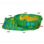
Warpage Calculation: Extract the maximum warpage value and distribution pattern from the out-of-plane displacement data.
Strain concentration zone identification: Identify the areas with the greatest strain during thermal deformation as potential failure points.
Temperature-deformation relationship modeling: Establishing an empirical formula for chip warpage as a function of temperature.
Comparison with simulation: Verify the material parameters and boundary condition settings of the finite element model.
FAQ
Q1: Can a micro-DIC chip measure its operating status?
A1: Yes, but you need to ensure that the optical system is compatible with the chip's operating environment, such as dust protection and anti-static properties.
Q2: How to maintain stable speckle patterns at high temperatures?
A2: High-temperature resistant ceramic speckle or laser etching marking can be used to avoid the effects of thermal oxidation.
Q3: How high is the measurement accuracy of chip warpage?
A3: With appropriate optical configuration, the accuracy of out-of-plane displacement measurement can reach the sub-micron level.
Q4: What are the advantages of micro-DIC compared to traditional interferometers?
A4: DIC requires no complex optical path adjustments, is highly adaptable, and can measure a larger field of view and complex surfaces.
Q5: What are the prospects for the application of micro-DIC in chip reliability testing?
A5: It has significant value in packaging design optimization, failure analysis, and lifetime prediction.