As the advanced packaging industry experiences rapid growth, thermal warpage has emerged as a critical bottleneck hindering yield improvements. The composite structure of chips—comprising multiple heterogeneous materials—leads to significant mismatches in the Coefficient of Thermal Expansion (CTE); micron-scale thermal warpage triggers issues such as micro-bump misalignment, delamination, cold joints, and chip cracking, resulting in substantial yield losses.
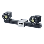
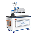
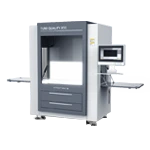
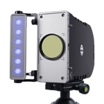
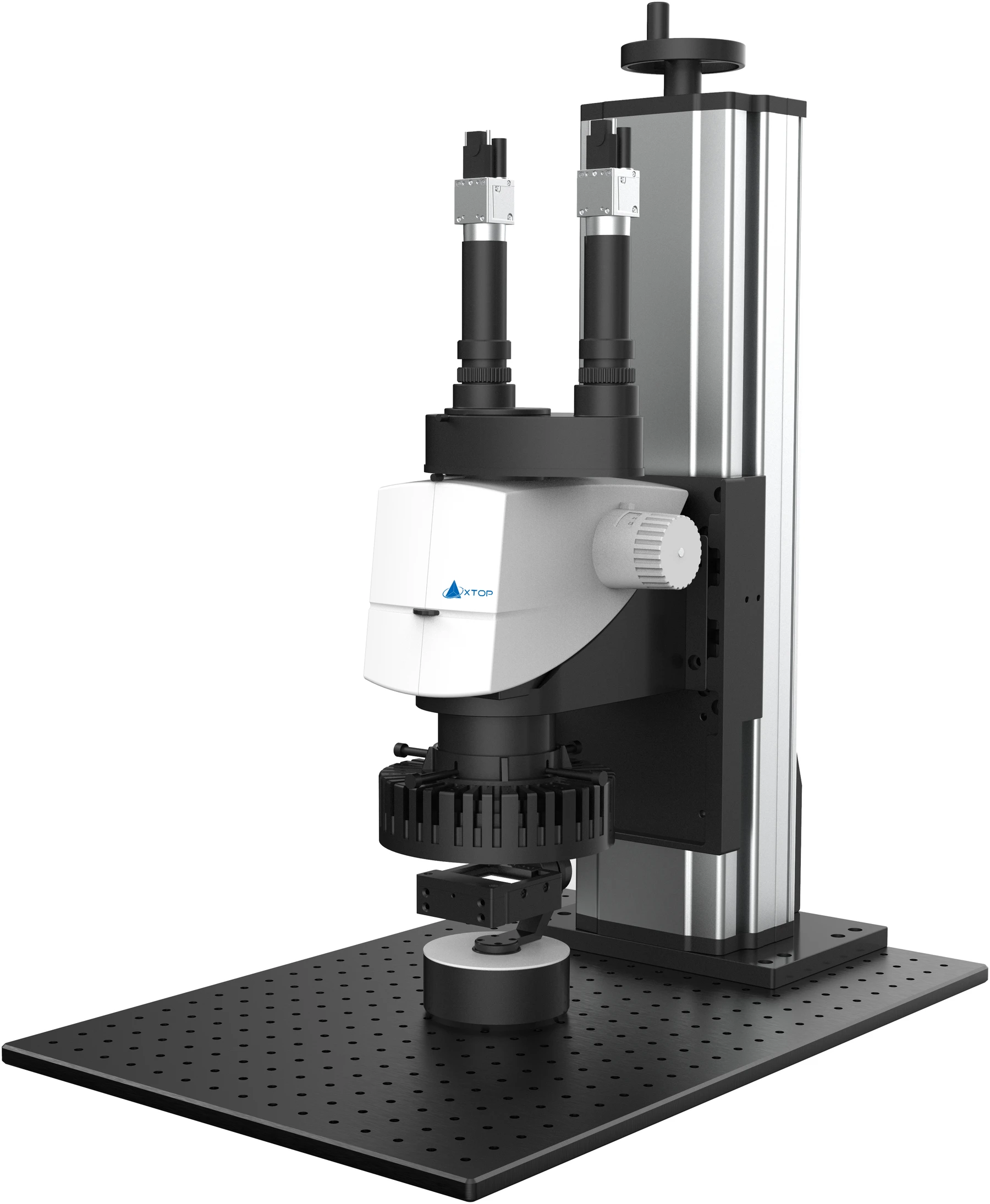
The XTOP3D microscopic DIC measurement system offers a standardized inspection solution covering the entire value chain—from chip design and packaging processes to reliability verification and failure analysis. It is designed for the quantitative analysis of micron-scale dynamic thermal warpage in advanced packaging, thereby supporting yield enhancement and technological evolution within the domestic advanced packaging industry.
Industry Data: Domestic advanced packaging capacity continues to expand, yet yield bottlenecks are primarily driven by thermal stress-induced deformation. Industry surveys indicate that 37.2% of early-stage failures on advanced packaging lines are caused by stress concentrations resulting from thermal warpage. Traditional single-point, single-dimensional inspection equipment is unable to quantify 3D deformation and thermal warpage, representing a critical shortcoming that constrains technological breakthroughs for domestic packaging and testing enterprises.
Three major pain points in the traditional testing equipment industry:
1. Only single Z-axis warping is measured, and interlayer planar slip and interface strain data are missing, making it impossible to analyze the stress coupling mechanism between 3D stacked layers;
2. It lacks microscopic magnification adaptation capability and cannot measure the deformation of micro-chips and interposers within 5mm.
3. Measurement errors are large under high and low temperature reflow soldering and thermal shock conditions, making it impossible to fully capture the warp peak during the entire dynamic heating and cooling process.
II. Thermal Warpage Deformation Analysis of Adaptor Chips for Microscopic DIC Measurement System
2.1 List of Advanced Packaging Subcategories
3D stacked packaging: PoP memory stacking, 3D IC logic memory stacking, multi-layer interposer chips;
HBM High Bandwidth Memory: Small stacked memory chips, micro-bump high-density interconnect package;
Fan-out packaging: Ultra-thin plastic-encapsulated substrate-free fan-out chip;
Chiplet heterogeneous integration: multi-chip splicing micro-package;
Automotive-grade advanced packaging: small power MCUs, SiC power micro-packages;
Traditional micro-packages: QFN, CSP, SSD controllers, SoC consumer electronics chips.
2.2 Advanced Packaging and Dedicated Testing Advantages
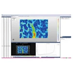
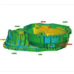
1. Visualization of interlayer strain in multi-layer stacking: Full-field strain cloud map can intuitively identify high-stress delamination risk areas at the stacking interface;
2. Micro-bump micron-level deformation: μm-level warping accuracy captures minute offsets in the coplanarity of micro-bumps;
Simultaneous CTE calculation for multiple materials: The coefficient of thermal expansion of silicon wafer, molding compound, substrate and underfill adhesive are calculated separately to optimize the matching scheme of heterogeneous materials;
Full-temperature-range thermal shock simulation: from -190℃ liquid nitrogen low temperature to 600℃ high temperature, covering the stringent reliability standards of automotive-grade and computing chips.
III. Five Major Application Scenarios of the Advanced Packaging Industry Chain
3.1 Chip Front-End Material and Structure Design Stage
Semiconductor design companies use micro-DIC to calculate the CTE parameters of different materials during the research and development stages of new packaging structures, new molding compounds, and underfill adhesives. This simulates the thermal cycling deformation of multilayer composite structures, helps avoid warpage failures caused by CTE mismatch in advance, reduces the number of tape-out iterations, and significantly lowers R&D costs.
3.2 Packaging process development and reflow soldering process optimization
Packaging and testing companies simulate complete reflow soldering temperature profiles, quantify the impact of heating rate, holding time, and peak temperature on chip warpage, optimize furnace temperature profiles, and reduce microbump soldering defects; for 3D stacked chips, they quantify the superimposed warpage deformation caused by the increase in the number of stacked layers and optimize the stacking process sequence.
3.3 Reliability Temperature Cycling Aging Verification (JESD22 Standard)
It meets the JEDEC temperature cycling reliability test standard, completes multiple rounds of continuous deformation data acquisition throughout the entire process of thermal shock, quantifies the cumulative plastic deformation of the chip under long-term cycling, assesses the reliability of the product throughout its entire life cycle, and the test data can be directly used for the issuance of third-party certification reports.
3.4 Batch Failure Analysis and FA Source Tracing
When batch delamination, poor soldering, or chip cracking occur on the production line, microscopic high and low temperature deformation tests are conducted on the failed samples to locate the high strain concentration areas at the four corners of the chip, the stacking interface, and the pads. This accurately identifies thermal warping as the root cause of the failure, and quickly provides a process improvement plan, shortening the failure analysis cycle by more than 70%.
3.5. Basic Research on Advanced Packaging in Scientific Research Institutes
The microelectronics and materials mechanics laboratories are used for research on 3D stacked thermal stress coupling, thermodynamic behavior of novel packaging materials, and stress mechanism of Chiplet heterogeneous integration. They output full-field quantitative strain data to support the publication of high-level papers and experimental data support for national key research and development projects.
IV. XDTIC-MICRO's Six Core Technologies Address Pain Points in the Advanced Packaging Microscopy High-Temperature Measurement Industry
Addressing six common industry errors in 3D stacking and HBM ultrathin microchip high and low temperature testing—namely, thermal airflow interference, bracket rigidity displacement, lens frost, depth-of-field drift, and microscopic calibration distortion—microscopic DIC measurement technology provides stable and reliable quantitative data for the advanced packaging industry.
Hot airflow suppression technology: isolates the interference of high-temperature rising airflow from reflow soldering, and eliminates systematic warping measurement deviation;
Rigid displacement elimination technology: automatically eliminates the overall displacement of the hot and cold stages and microscope supports due to thermal expansion, and only retains the true local deformation between chip layers;
Fogging and frosting suppression technology: high and low temperature sealed dry cavity, no frosting obstructing imaging at -190℃;
Full-range temperature compensation algorithm: Automatic correction of lens distortion in different temperature ranges, with a stable accuracy of 0.1μm across the entire temperature range;
Automatic microscopic calibration technology: One-click correction of microscope lens distortion, eliminating manual calibration errors;
Ultra-depth dynamic compensation technology: The ultra-thin chip heats up and warps, causing height shifts, and automatically focuses, ensuring clear images without going out of focus throughout the entire process.
V. The Industrial Value of Domestically Produced Micro-DIC Equipment: Breaking the Monopoly of Imported Testing Instruments
In the past, China's high-end advanced packaging thermal deformation microscopic inspection equipment relied heavily on imported equipment, resulting in high procurement costs, long after-sales response cycles, and software that was not compatible with the customized reflow soldering profiles of domestic packaging and testing companies. The domestically produced microscopic DIC measurement system, however, achieves fully independent software and hardware development and possesses three major industrial values:
Cost advantage: The purchase price of the whole machine is more than 40% lower than that of imported similar micro DIC equipment, which greatly reduces the investment threshold for laboratory testing equipment;
Localized services: Agile technical support from domestic technical teams to quickly adapt to the customized testing needs of domestic hot and cold testing stations and packaging and testing production lines;
Open and compatible data: The DIC software has an open data export interface, which can be connected to FEA simulation software and MES production line data system, adapting to the digital transformation needs of domestic semiconductor intelligent manufacturing.
VI. Industry Development Trends: Microscopic DIC Technology Becomes a Standardized and Essential Testing Equipment for Advanced Packaging
Industry standards are being improved: JEITA and IPC semiconductor packaging deformation testing standards are gradually adding requirements for full-field three-dimensional strain and CTE quantitative testing, and single Z-axis warpage measurement cannot meet the new standards;
Pre-R&D Testing: More and more packaging and testing companies are moving micro-DIC deformation testing to the material selection and structural design stages to control thermal warpage failure from the source, rather than tracing the source after production line defects occur;
Digital simulation linkage: The measured deformation data of microscopic DIC is benchmarked with digital twins and FEA simulation to build a closed loop of digital R&D for advanced packaging, becoming a core testing tool.
VII. FAQ for Industrial Clients
Q1: Can you measure ultra-thin fan-out substrate-free packaged chips?
A: It is compatible with 1–10mm microscopic field of view and μm-level warp accuracy, and can accurately measure the micron-level bending deformation of ultra-thin plastic sealant.
Q2: Can the measurement accuracy of domestically produced micro DIC equipment match that of imported brands?
A: Z-axis warping accuracy at the μm level and strain accuracy at 20με. The repeatability of measured data and stability across the entire temperature range are comparable to imported micro DICs. Furthermore, it is compatible with domestic reflow soldering process curves, demonstrating stronger localization capabilities.
The domestic advanced packaging industry has entered a period of rapid expansion, and material thermal warpage has become a core bottleneck restricting production line yield and product reliability. The microscopic DIC deformation measurement system covers the entire advanced packaging industry chain, from material design, process development, reliability verification to failure analysis. It achieves simultaneous quantitative detection of micron-level three-dimensional warpage, full-field strain, and CTE thermal expansion coefficient, providing a standardized optical measurement solution for technological iteration and yield improvement in the domestic semiconductor advanced packaging industry.