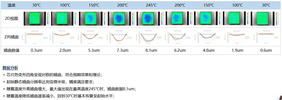
This study analyzes the thermal deformation of a 4.5 × 4.5 mm packaged chip during a full-temperature reflow cycle. Using a microscopic DIC measurement system, warpage data was captured throughout the heating and cooling process (30°C to 245°C), quantifying a peak symmetric warpage of 8.1 μm and confirming that high-temperature, micron-scale warpage is the primary cause of batch failures due to micro-bump cold joints. The standardized operational workflow, spanning from sample preparation to final data acquisition, is fully demonstrated.
A mass-production challenge faced by an electronics packaging and testing plant involved a specific chip model that exhibited a ~12% defect rate—specifically "cold" (incomplete) solder joints and open circuits—following the standard reflow soldering process. Conventional single-point height gauges could only measure static warpage at room temperature; they failed to capture dynamic deformation at the 245°C peak temperature or pinpoint the root cause of the failure.
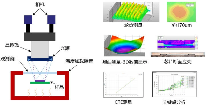
By employing a microscopic DIC (Digital Image Correlation) measurement system to conduct full-cycle thermal simulation testing, the team successfully replicated the deformation dynamics across the entire reflow process—including heating, soaking, and cooling phases. They precisely quantified warpage values at various temperature points and optimized both the molding compound formulation and the reflow heating profile, ultimately reducing the defect rate to below 0.8%.
I. Basic Parameters of the Sample
Package type: Leadless quad flat package
Chip size: 4.5mm × 4.5mm × 0.5mm
Test temperature range: 30℃ (room temperature starting point) → 100℃ → 150℃ → 200℃ → 245℃ (reflow soldering peak), with segmented cooling back to 30℃.
Constant temperature insulation rule: After holding at each temperature node for 5 minutes, collect three-dimensional deformation data to simulate the industrial reflow soldering insulation process.
Measurement field of view: 5mm, matching the standard measurement range of the micro-dic measurement system.
II. Practical Steps for Hardware Setup and Preliminary Preparations for the Complete Testing System
2.1 Hardware Equipment List (Case Study Site Configuration)
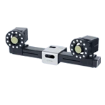
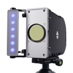
XTDIC-MICRO 3D Microscopic Strain Measurement System: Dual industrial synchronous cameras, 10x body microscope, and ring stroboscopic low-noise light source;
Programmable high and low temperature heating and cooling stage: temperature control range -190℃~600℃, temperature accuracy ±0.1℃;
Automatic microscopic calibration plate, high-temperature speckle pattern preparation kit, heat-insulated sealed cavity;
DIC analysis software and FEA simulation data interface module;
Vibration isolation test bench (to eliminate image jitter errors caused by environmental vibration).
2.2 Sample Pretreatment Practical Steps
Chip surface cleaning: Wipe the plastic-encapsulated surface with anhydrous ethanol to remove oil and dust, ensuring the adhesion of speckles;
High-temperature resistant speckle spraying: uniformly spray black and white random micro speckles, with speckle diameter matching the microscope lens pixels, and air dry for 10 minutes.
Sample clamping: The sample is placed flat and fixed on the ceramic stage of the hot and cold table, without mechanical compression, to avoid pre-deformation of the clamping interfering with the measurement;
Cavity sealing treatment: Close the insulation door, start the drying and anti-fog air duct, and pre-circulate for 5 minutes to eliminate temperature difference and water vapor in the cavity.
2.3 Calibration Operation of Microscopic DIC Measurement System (One-Click Automated Process)
Place the special photolithography calibration plate for microscopy on the same plane as the sample, start the automatic calibration program in the software, and complete the binocular camera distortion correction, microscope magnification compensation, and baseline stereo parameter calibration in 5 minutes. After calibration, save the calibration parameters and reuse the entire test process.
III. Programming and Synchronous Acquisition Settings for Reflow Soldering Step Temperature Profile
3.1 Standardized temperature loading procedure (industry-standard reflow soldering simulation curve)
Phase 1: Initial room temperature 30℃, constant temperature for 5 min, and acquisition of baseline zero deformation image;
Phase 2: Heat to 100℃ at a constant rate, hold for 5 minutes, and then trigger image acquisition;
Phase 3: Heat to 150℃, hold for 5 minutes, and collect data;
Phase 4: Heat to 200℃, hold for 5 minutes, and collect data;
Phase 5: Heat to the reflow soldering peak temperature of 245℃, hold for 5 minutes, and collect data on the maximum deformation at high temperature;
Cooling phase: 200℃→150℃→100℃→30℃, hold each node for 5 minutes and acquire images simultaneously;
Cyclic setting: Supports multiple rounds of repeated hot and cold cycle tests to simulate long-term temperature aging conditions.
3.2 Synchronous Acquisition Parameter Settings
The dual-camera synchronous stroboscopic exposure lasts 1ms, eliminating image trailing in high-temperature hot airflows; each temperature insulation node automatically triggers the capture of 20 sets of speckle images, and the software averages them to reduce random measurement noise and ensure the repeatability of warpage values.
H2
IV. Complete Measured Data Results and Deformation Pattern Analysis (PPT Original Measured Data Table)
4.1 Summary table of maximum Z-axis warpage values at each temperature node
|
Temperature node
|
30℃
|
100℃
|
150℃
|
200℃
|
245℃ (peak temperature)
|
200℃ cooling
|
150℃ cooling
|
100℃ cooling
|
30℃ endpoint
|
|
Maximum Z-axis warpage of the chip
|
0.3μm
|
2.0μm
|
5.3μm
|
7.3μm
|
8.1μm
|
6.2μm
|
4.8μm
|
1.9μm
|
0.6μm
|
4.2 Interpretation of the Core Laws of Deformation
Deformation symmetry characteristics: The four corners of the chip warp upwards synchronously, exhibiting a standard bowl-shaped symmetrical deformation, which conforms to the theoretical model of thermal expansion coefficient mismatch of QFN package multilayer materials, with no local abnormal offset;
Temperature positive correlation law: As the temperature continues to rise, the warpage value increases linearly. The reflow soldering peak temperature reaches 245℃, where the maximum deformation is 8.1μm, which is the temperature range where welding defects are prone to occur.
Cooling rebound reversibility: During the cooling process, the warpage gradually decreases, and only a tiny permanent deformation of 0.6μm remains when it returns to room temperature of 30℃. This indicates that the thermoelastic deformation of the encapsulation material is dominant, and the plastic deformation accounts for a very low proportion.
Static reference accuracy: The initial warpage at room temperature of 30℃ is only 0.3μm, and the submicron level accuracy of the system fully meets the requirements for static deformation detection of micro-packages.
4.3 Software Visualization Data Output Content
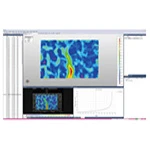
A full-temperature-range 2D warped grayscale cloud map visually displays the height distribution on the chip surface;
The Z-axis warping polygonal line diagram of the central section is used to extract the diagonal deformation curve of the chip.
The overall principal strain distribution cloud map identifies high strain concentration areas in the four corner pad regions of the chip.
The temperature-maximum warpage correlation data table can be directly exported for use in process reports.
V. Test Data Implementation and Process Improvement Plan (Case Study Value)
Based on the quantitative data from this full-process test of micro-DIC, the company simultaneously implemented three process optimization measures, significantly reducing the welding defect rate:
Optimization of molding compound material: Replace with low CTE matching molding compound resin to reduce the thermal expansion difference between silicon wafer and molding compound layer, reducing the 245℃ peak warpage from 8.1μm to less than 4μm;
Reflow soldering temperature rise profile adjustment: slow down the temperature rise rate of 180℃–245℃ to reduce instantaneous thermal stress shock and reduce instantaneous warpage peak;
Substrate thickness fine-tuning: Appropriately increasing the substrate thickness improves structural rigidity and suppresses overall bending deformation at high temperatures.
After optimization, the peak warpage of the second micro-DIC test was reduced to 3.7μm, and the defect rate of poor soldering on the production line decreased from 12% to 0.8%, verifying the core guiding value of the dynamic temperature warpage test of micro-DIC for packaging process improvement.
VI. Case Extension to Adapt to More Chip Package Types
The 4.5mm QFN case test solution can be directly adapted to mainstream micro-packages:
Consumer electronics: CSP, PoP stacked storage chips, SSD controller chips;
Computing chips: small GPUs, SoC packages;
Automotive-grade semiconductors: small MCUs, power device packaging;
Advanced packaging: Fan-out, Chiplet miniature interposer chip.
Only the microscope magnification and hot/cold stage fixture need to be finely adjusted according to the chip size; the testing process and data output logic are completely universal.
VII. Common Questions and Answers in Practical Engineering (FAQ)
Q1: What is the reason for the poor repeatability of chip warpage values during testing?
A: It is highly likely that the cavity was not open for anti-fog airflow, or that hot airflow was interfering, or that rigid displacement correction was not performed. Activating the two core patented technologies of the device will stabilize the data repeatability.
Q2: How to solve the blurring of speckle images at a high temperature of 245℃?
A: Activate the super depth-of-field compensation technology, and the software will automatically focus in real time. At the same time, activate the hot airflow suppression channel to eliminate image distortion caused by high-temperature air refraction.
Q3: Can the warpage data obtained from the test be directly used in a third-party reliability report?
A: XTOP software outputs raw, unaltered quantitative data, cloud maps, and temperature time-series curves. The data has complete traceability and can be directly used as valid data support for packaging and testing reliability test reports.
Q4: How long does a single complete reflow soldering cycle test take?
A: The entire process, including heating, holding, and cooling, takes about 90 minutes. The data is collected automatically throughout the process, requiring no manual intervention. Batch samples can be continuously tested in cycles.
This case study of reflow soldering thermal cycling fully implements a standardized testing process for micro-DIC technology. It quantifies and reconstructs the micron-level thermal warpage changes of the chip throughout the entire reflow soldering peak process from room temperature to 245°C, accurately identifying the maximum deformation of 8.1μm at high temperature as the core cause of batch soldering failures. The entire testing solution features simple hardware setup, high automation, and intuitive data quantification. It can be directly replicated and applied to process verification, failure analysis, and new material development for various micro-semiconductor packages, providing advanced packaging companies with a practical and standardized solution for quantitative thermal warpage detection.