Industry statistics indicate that over 50% of semiconductor component failures stem from thermal stress caused by temperature fluctuations and chip thermal warpage; the proportion of defects attributable to thermal deformation far exceeds the combined total of failures caused by vibration, humidity, dust, and other factors. As chip packaging structures evolve toward miniaturization and multi-layer composite designs, significant mismatches in the Coefficient of Thermal Expansion (CTE) arise among the diverse materials involved—such as silicon wafers, molding compounds, organic substrates, micro-bumps, and underfill materials.
Under conditions ranging from peak reflow soldering temperatures of 245°C and cryogenic shocks in liquid nitrogen (-190°C) to thousands of JEDEC-standard thermal cycling stress tests, even minute warpage can trigger mass-production yield issues, including micro-bump cold joints, "head-in-pillow" defects, solder bridging, package delamination, and chip cracking. Traditional inspection equipment—such as single-point altimeters, Shadow Moiré (SM), White Light Interferometry (WLI), and Digital Fringe Projection (DFP)—faces inherent limitations when applied to micro-scale packaging: they typically capture only Z-axis warpage height without providing data on in-plane displacement, full-field strain, or material CTE. Furthermore, they suffer from poor compatibility with microscopic fields of view and significant measurement errors caused by thermal air currents, lens frosting, and rigid-body equipment displacement in extreme temperature environments. Consequently, they fail to fully characterize the dynamic thermal deformation patterns of chips throughout the process, severely hindering material selection, process optimization, and the efficiency of failure analysis in advanced packaging.
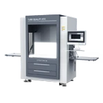
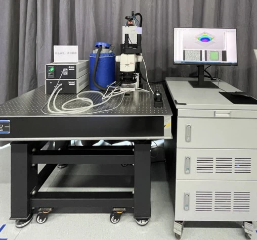
To address these industry challenges, Micro-DIC (Digital Image Correlation) measurement technology has emerged. With core advantages—including non-contact operation, sub-micron precision, multi-dimensional data output, and stability across the entire temperature range—it has become the standardized technical approach for the quantitative inspection of chip thermal warpage, deformation, and stress. Representative systems, such as the XTOP3D XTDIC-MICRO, comprehensively meet inspection requirements across the entire value chain, spanning chip R&D, packaging processes, reliability verification, and failure analysis.
I. Principle of Microscopic DIC Technology: Fusion of Binocular Microscopic Vision and Digital Image Correlation Algorithm
Microscopic DIC technology is a deep integration of binocular stereoscopic optical imaging and DIC digital image correlation speckle tracking algorithm. It is specifically developed for the measurement of microscale deformation of 1–10mm microchips. Unlike ordinary macroscopic DIC large field-of-view devices, it integrates a 10x optical microscopic magnification module to achieve the capture of micron and submicron level micro-deformations.
1.1 Principle of Binocular Stereo Vision 3D Reconstruction
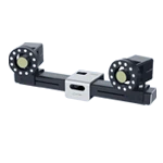
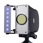
The system is equipped with two synchronous industrial cameras to form a fixed observation baseline, and uses a stereomicroscope to simultaneously acquire images of the chip surface. A high-precision microscopic calibration plate automatically corrects lens distortion, magnification, and baseline parameters. It performs stereo matching of speckle feature points on the chip surface captured by the left and right cameras, accurately calculates the three-dimensional spatial coordinates of each pixel, constructs a complete three-dimensional contour model of the chip, and synchronously outputs X (lateral), Y (vertical), and Z (warp height) three-dimensional full-field coordinates. This accurately captures all deformation behaviors of the chip, including vertical bending and planar slippage, overcoming the core deficiency of traditional two-dimensional measurements that cannot obtain the warp height.
1.2 Principle of DIC Digital Image Correlation Speckle Tracking Algorithm
Before testing, high-temperature resistant random micro-spots are sprayed onto the chip surface as unique identification features for the algorithm. The system acquires original images of the room temperature baseline as reference templates, and simultaneously acquires sample images at each constant temperature node of heating, holding, and cooling. The algorithm compares the speckle position offset in the two images pixel by pixel, calculates the X and Y plane displacements of all points on the chip surface, and further derives the Z-axis out-of-plane warping displacement by combining binocular three-dimensional coordinates.
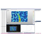
Based on the displacement gradient differential algorithm, the software automatically generates full-field principal strain and shear strain visualization cloud maps, intuitively marking the high stress concentration areas at the four corners of the chip, the pads, and the interlayer interfaces; at the same time, it automatically calculates the CTE thermal expansion coefficient of the packaging material through multi-temperature displacement data, quantitatively judges the degree of CTE mismatch of multilayer materials, and analyzes the thermal warpage failure mechanism from the root.
1.3 Standardized Complete Process for Chip Thermal Cycling Test
· Sample pretreatment: Clean the chip surface and spray with high-temperature resistant micro-spot coating, which is suitable for long-term observation at 245 ℃ reflow soldering without falling off;
· Automatic calibration of the microscopic DIC measurement system: Place a special photolithography calibration plate for microscopy, and the software will complete the full optical path distortion correction with one click, eliminating manual calibration errors;
· Sample clamping and cavity sealing: The chip is fixed on the programmable hot and cold stage, the heat-insulated drying cavity is closed, and the anti-fog and heat-insulated air duct is activated to avoid high and low temperature frost and hot air flow interference.
· Temperature profile programming and synchronous acquisition: replicate the standard reflow soldering curve ( 30 ℃ → 100 ℃ → 150 ℃ → 200 ℃ → 245 ℃, segmented cooling back to room temperature), and automatically trigger image acquisition after holding at each temperature node for 5 minutes ;
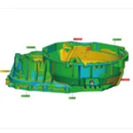
· Multi-dimensional data post-processing output: XTOP analysis software automatically outputs warp contour plots, Z -direction deformation values, full-field strain distribution, temperature - warp time series curves, and CTE parameters, and supports direct data connection to FEA finite element simulation software to complete calibration.
III. Core Differentiating Advantages of Microscopic DIC Measurement Technology
The current mainstream thermal warp detection technologies in the semiconductor industry include four types: DIC, SM shadow moiré, DFP digital stripe projection, and WLI white light interferometry. A horizontal comparison from five dimensions—measurement dimensions, accuracy, microscopic adaptation, full-temperature stability, and data integrity—shows that only microscopic DIC can achieve full-dimensional three-dimensional full-field synchronous measurement, while the other technologies all have key capability deficiencies.
Summary of the core advantages of microscopic DIC measurement technology
1. The only full-dimensional measurement solution: Simultaneously acquires five core data categories: three-dimensional coordinates, XY plane displacement, Z-axis warping, full-field strain, and CTE, with a single device replacing multiple sets of traditional testing instruments;
2. Non-contact non-destructive testing: No probes, no mechanical contact, will not scratch the pads of microchips and the surface of the plastic package, and valuable R&D samples can be repeatedly tested in cycles;
3. Submicron ultra-high measurement accuracy: Z-axis warp measurement accuracy can reach 0.1μm, strain measurement accuracy is 20με, which fully matches the advanced packaged micron-level deformation detection standard;
4. Full temperature range coverage: Equipped with a programmable hot and cold stage, it covers liquid nitrogen extreme low temperature -190℃ to high temperature 600℃, perfectly simulating reflow soldering, thermal shock, and high temperature aging conditions.
5. Two-way communication of simulation data: The measured full-field deformation and strain data can be directly imported into the FEA simulation software to correct the simulation model parameters and open up the "simulation-measurement" R&D closed loop.
IV. Self-developed core anti-interference technology solves the challenges of high and low temperature measurement.
Conventional DIC equipment used for high and low temperature microscopic testing of chips can suffer from systematic errors such as thermal airflow refraction drift, rigid displacement of the support, lens frost, sample defocusing, and calibration distortion. The XTDIC-MICRO microscopic DIC measurement system from Newtop 3D can avoid measurement interference from microscopic temperature variations and ensure long-term stable and reproducible data.
1. Hot airflow suppression technology: The closed constant temperature circulating air duct isolates the rising heat convection of the hot and cold platforms, eliminates the regular image shift caused by the air refractive index gradient, and reduces the warp measurement system error from ±3μm to within ±0.1μm;
2. Rigid displacement elimination technology: The algorithm automatically separates the overall rigid displacement caused by the thermal expansion and contraction of the hot and cold stages and microscope support, retaining only the true local deformation of the chip, and avoiding the misjudgment of thermal expansion of the equipment as sample warping;
3. Fogging and frosting suppression technology: The chamber is continuously replaced with dry nitrogen gas, and water vapor is isolated throughout the high and low temperature process. There is no frosting at -190℃ and no fogging at 245℃, and the image is clear and can be acquired throughout the process.
4. Full-range temperature compensation algorithm: Built-in multi-temperature range lens distortion correction database, dynamically corrects pixel coordinate drift according to real-time temperature, and maintains stable measurement accuracy across the entire temperature range;
5. Automatic microscopic calibration technology: The backlit photolithography calibration plate is automatically identified and calibrated, eliminating magnification deviation caused by manual focusing, and the repeatability error of repeated measurements is <0.05μm;
6. Ultra-depth-of-field dynamic compensation technology: Real-time monitoring of sample speckle clarity, automatic fine adjustment of microscope focus height, chip heating warping shift does not deviate from effective depth of field throughout the process, eliminating image defocus and data loss.
V. Application Scenarios of Microscopic DIC Measurement Technology
5.1 Front-end material and packaging structure research and development
Semiconductor design and material manufacturers use it to verify the thermodynamic properties of new molding resins, substrates, and underfill adhesives. By using a microscopic DIC measurement system to accurately calculate the CTE parameters of different materials, the system can simulate the thermal cycling deformation of multilayer composite structures, avoid warpage failures caused by CTE mismatch in advance, significantly reduce the number of tape-out iterations, and lower the cost of R&D trial and error.
5.2 Optimization of Packaging Reflow Soldering Process
Simulate the complete temperature profile of reflow soldering from 30℃ to 245℃, a standard industrial standard, quantify the impact of heating rate, holding time, and peak temperature on chip warpage, and optimize the furnace temperature profile; adjust the stacking process and bottom fill curing parameters to address the cumulative deformation caused by advanced packaging stacking.
5.3 JEDEC Standard Reliability Temperature Cycling Verification
It meets automotive-grade and computing chip thermal shock and long-term temperature aging test standards, automatically completes continuous deformation data collection under thermal cycling, quantifies the cumulative plastic deformation of the chip under long-term cycling, assesses the reliability of the product throughout its entire life cycle, and the complete data can be directly used for the issuance of third-party testing and certification reports.
5.4 Production Line Batch Failure Analysis (FA)
When production lines experience batch defects such as delamination, poor soldering, or chip cracking, microscopic high and low temperature deformation tests are conducted on the failed samples. By using full-field strain cloud maps, high stress concentration areas such as the four corners of the chip, interlayer interfaces, and solder joints can be quickly located, accurately identifying thermal warping as the root cause of failure. This shortens the failure tracing cycle by 70% and quickly outputs feasible process improvement solutions.
5.5 Basic Research in Universities and Research Institutes
The microelectronics and materials mechanics laboratory is used for the study of 3D stacked thermal stress coupling, MEMS microdevices, and the thermodynamic mechanism of novel packaging materials. The full-field quantitative strain data can directly support academic papers and experimental verification of national key R&D projects, and is a standard equipment for microscopic semiconductor mechanical testing.
Under the major industrial trends of advanced packaging miniaturization, high reliability, and domestic substitution, traditional single-dimensional, low-precision, and poorly temperature-range adaptable testing equipment can no longer meet the full-process testing requirements of chip thermal warpage. The microscopic DIC measurement system integrates binocular microscopic vision and digital image correlation algorithms, combined with six self-developed high and low temperature anti-interference technologies, to achieve simultaneous quantitative measurement of 1–10mm microchips across the entire temperature range of -190℃ to 600℃, three-dimensional full-field warpage, displacement, strain, and CTE, filling the industry gap in high-precision detection of dynamic thermal deformation of micro-packages.
From materials research and development, process iteration, reliability verification to failure analysis, the micro- DIC measurement system comprehensively covers the needs of semiconductor packaging thermal warpage deformation detection. Simultaneously, relying on localized technical services, it rapidly responds to the customized reflow soldering and thermal shock testing needs of packaging and testing companies, becoming a core optical measurement tool for the advanced packaging industry to improve yield, shorten R&D cycles, and overcome technical bottlenecks in thermal stress deformation.