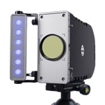
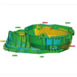
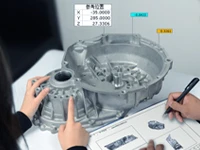
With the development of micro-nano manufacturing technology, micro-sized materials (micrometer to millimeter scale) are increasingly widely used in aerospace, microelectromechanical systems (MEMS), precision instruments and other fields. Compared with traditional macro-sized materials, the mechanical behavior of micro-sized materials exhibits a significant size effect —that is, the strength, plasticity, fracture toughness and other properties of materials at the micro-scale are different from those in the macro-scale state.
With its high spatial resolution and non-contact full-field measurement capabilities, the micro-DIC strain measurement system has become an ideal tool for studying the mechanical properties of small-sized materials.
I. Challenges in the Research of Micro-sized Materials
Size effect is significant: grain size and defect distribution have a greater impact on mechanical properties.
Traditional sensors are not suitable: strain gauges and extensometers are difficult to install on tiny samples.
Loading control is difficult: small samples are easily damaged during clamping or loading.
High measurement accuracy is required: the strain change amplitude is small, requiring submicron or even nanometer resolution.
II. Technical Advantages of Micro-DIC
Non-contact measurement: Avoids the influence of sensor added stiffness on sample deformation.
Full-field data: The displacement and strain distribution of the entire sample surface can be obtained in a single experiment.
High resolution: When used with a high-powered microscope, the spatial resolution can reach 0.1 micrometers per pixel.
Multiscale analysis: Different magnifications can be switched within the same system to enable cross-scale research.
III. Typical Application Cases
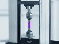
1. Tensile testing of microfilaments and microbeams
Metal wires or silicon microbeams with diameters of tens of micrometers can be precisely measured for their elastic modulus, yield strength, and fracture strain under micro-DIC.
2. Bending and peeling of thin film materials
Even with a film only a few micrometers thick, DIC can capture localized strain concentrations and crack propagation during bending or peeling.
3. Microcolumn compression experiment
Micropillar compression is a common method for evaluating the plastic behavior of small materials, and DIC can provide information on strain evolution during the compression process.
4. Interfacial Mechanics of Multimaterial Microstructures
For example, the analysis of interfacial strain distribution in metal-ceramic microstructures under thermal or mechanical loads.
IV. Key Points of Experimental Design and Implementation
Sample preparation: The size of the surface speckle should match the sample size to avoid affecting the mechanical behavior.
Loading device: A micro-force loading stage is used, and the loading accuracy can reach the millinewton level.
Environmental control: shockproof, temperature-controlled, and dustproof to ensure measurement stability.
Data acquisition: Select the appropriate camera frame rate and exposure time according to the experimental requirements.
V. Data Analysis and Results Interpretation
The displacement and strain fields output by the micro-DIC can be used for:
Calculate the elastic modulus and Poisson's ratio.
Analyze the yielding behavior and hardening properties.
Evaluate fracture toughness and crack propagation path.
Verify the accuracy of the micromechanical model.
FAQ
Q1: Can micro-DIC be used to measure nanoscale materials?
A1: It can directly measure micron-scale materials, while nanoscale materials require multi-scale analysis using atomic force microscopy (AFM) or scanning electron microscopy (SEM).
Q2: How are speckle patterns prepared for small samples?
A2: Nanoparticle deposition, electron beam etching, and other methods can be used to ensure that the speckle size is much smaller than the sample feature size.
Q3: How to verify the measurement accuracy of micro DIC?
A3: Calibration can be performed using standard samples with known displacements, or by comparison with other measurement methods.
Q4: What are the main sources of error in testing small-sized materials?
A4: This includes optical distortion, sample alignment error, environmental vibration, poor speckle quality, etc.