Printed Circuit Boards (PCBs) serve as the fundamental platform for electronic devices, fulfilling the dual roles of electrical interconnection and physical support: they facilitate circuit connectivity while securing electronic components such as resistors, capacitors, and microchips. Thanks to their significant advantages in terms of lightweight and compact design, PCBs are integral to virtually all electronic devices.
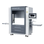
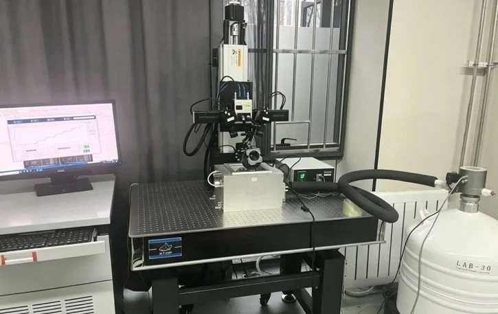
Under high-temperature operating conditions, PCBs and soldered components are prone to thermal deformation caused by mismatches in the Coefficient of Thermal Expansion (CTE), which can lead to reliability issues such as solder joint fatigue and connection failure. Consequently, thermal load testing has become a critical step in evaluating the in-service performance of PCBs. In this case study, the XTOP3D XTDIC 3D full-field strain measurement system is utilized to quantitatively analyze the impact of thermal loads on the deformation of the PCB and its mounted components, thereby providing data to support reliability-focused design.
I. Measurement Bottlenecks in Conventional DIC
Refraction Interference from Hot Air Turbulence
Heated air convection and temperature gradients around the PCB cause non-uniform air refractive indices. This leads to "virtual" or noise-induced displacements in the speckle images captured by DIC cameras, resulting in distorted strain and warpage data.
Thermal Environment Interference
High-temperature air disturbances cause image distortion, thermal radiation degrades speckle coating performance, and the equipment itself is subject to thermal drift errors.
Refraction-Induced Distortion
Installing heat-insulating glass in conventional DIC setups introduces refraction distortion, further increasing matching errors and distorting the calculated strain and warpage data.
Thermal Expansion Errors from Temperature Fluctuations
Rapid heating and cooling rates within the oven cause thermal expansion and contraction in the support structures, fixtures, and mounting stages. Conventional DIC struggles to distinguish between the overall displacement of the tooling and the actual deformation of the PCB itself.
II. DIC Measurement Solution
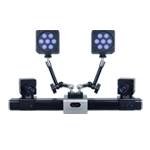
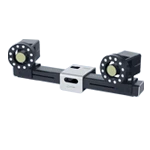
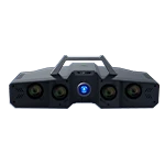
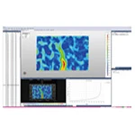
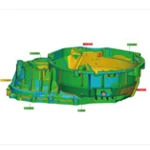
The XTDIC 3D full-field strain measurement system employs technologies such as high-temperature resistant speckle patterning, algorithms for the automatic elimination of rigid-body displacement, and distortion correction modules for observation windows. It accurately analyzes in-plane displacement, in-plane strain, and out-of-plane (Z-axis) warpage displacement on the circuit board. It extracts data on maximum deflection, overall twist, and localized bulging or depression, enabling the analysis of mechanisms by which warpage induces component placement shifts.
Ensuring Measurement Accuracy in Thermal Environments
-
Actively Temperature-Controlled Optical Window: A quartz glass viewing window combined with a closed-loop cooling system maintains the surface temperature below 50°C, eliminating refraction distortion caused by hot air currents
-
High-Temperature Resistant Speckle Pattern:Alumina-based ceramic coating (temperature resistance >300°C) with a particle size of 2–5 μm; speckle stability exceeds 99% at high temperatures.
-
Real-Time Thermal Drift Compensation: Position correction algorithm based on fixed ceramic reference points inside the high-temperature chamber; drift error is kept below 0.5 μm.
-
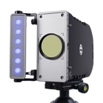
Multi-Band LED Cold Light Source:Narrow-band filters installed in front of the cameras suppress thermal radiation interference, significantly improving the signal-to-noise ratio. Automatic Rigid-Body Displacement Removal Algorithm: Leveraging a global reference point calculation logic, the DIC software isolates the PCB's true 3D deformation field, ensuring greater data consistency across high/low-temperature cycling and multi-batch repeatability tests.
III. PCB Thermal Warpage Measurement
1. Pre-test Preparation
Speckle Pattern Application: Spray high-temperature-resistant speckle paint onto the PCB's area of interest (the black section), ensuring the pattern neither peels nor fades at 125°C;
System Calibration: Rapidly calibrate the XTDIC 3D full-field strain measurement system (binocular setup) at room temperature to obtain initial intrinsic and extrinsic parameters;
Thermal Drift Pre-calibration: Calibrate the system against the temperature profile within the software to establish a drift compensation model;
Specimen Mounting: Place the PCB horizontally on the support rack inside the high-temperature chamber, ensuring boundary conditions that allow for free deformation.
2. Temperature Control and Data Acquisition
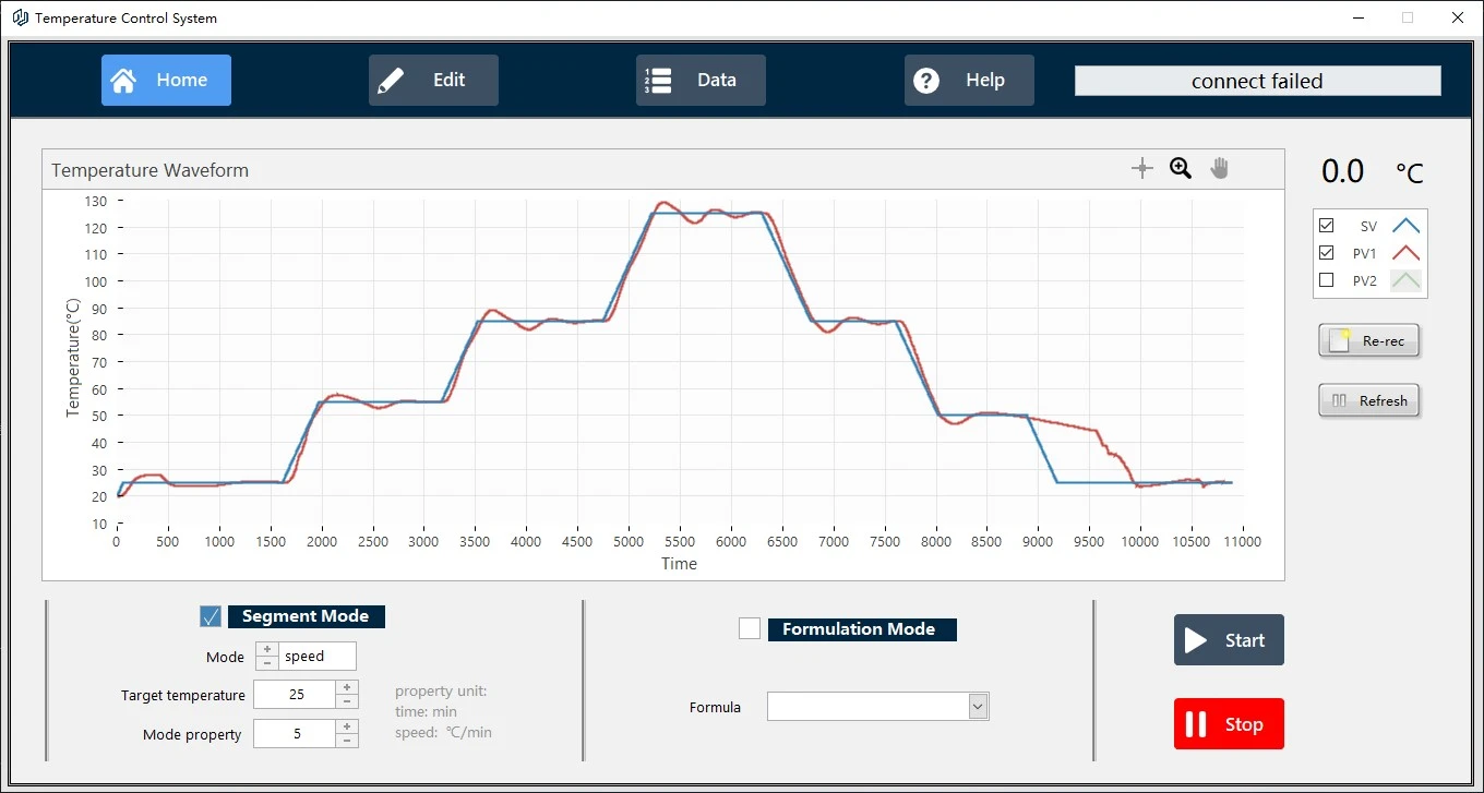
The test employs a temperature control strategy consisting of stepped heating, isothermal holding, and cooling phases:
Room temperature (baseline state) → 85°C (hold) → Maximum temperature 125°C (hold) → Room temperature (recovery state)
At each temperature setpoint:
Wait for the chamber temperature to stabilize (fluctuation < ±0.5°C); activate LED lighting and adjust brightness for optimal imaging;
Synchronously capture images using the binocular cameras and perform multi-frame averaging; execute the thermal drift correction algorithm in real-time to output the corrected 3D topography.
3. Test Results and Analysis
Displacement Distribution at Critical PCB Locations
The XTDIC 3D strain measurement system captured the full-field 3D displacement distribution of the PCB under the following four temperature conditions:
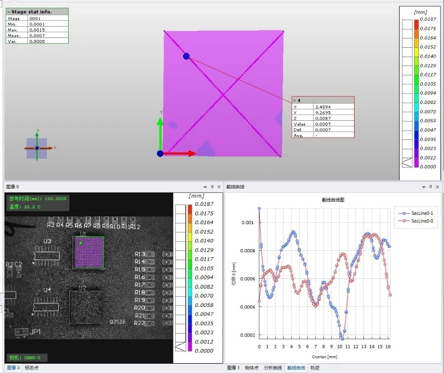
Room temperature (baseline)
Serving as the zero-displacement reference, the displacement map below shows the initial flat state, with a single-point displacement standard deviation of <0.3 μm.
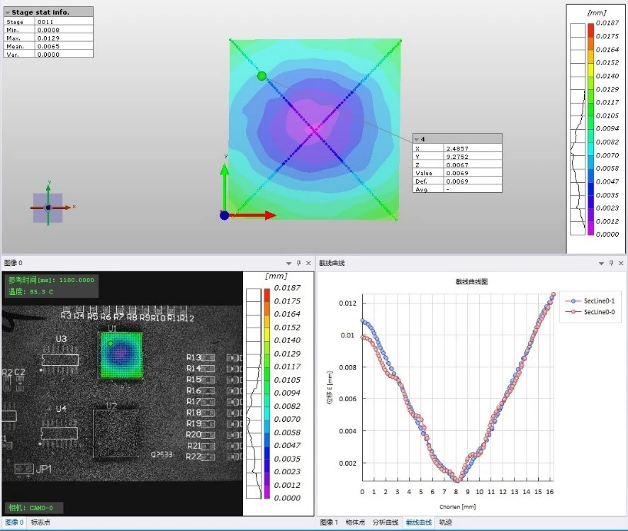
At a temperature of 85°C, significant thermal expansion and warping occur upon heating; the central region of the panel bulges into a "bowl" shape, with a maximum displacement of approximately 15 μm.
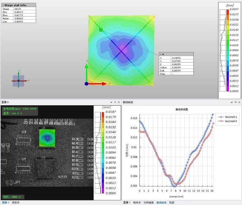
At a temperature of 125°C (the maximum temperature), warpage reaches its peak; the displacement in the central region increases to approximately 35 μm, while the edge regions exhibit reverse bending due to constraints.
Upon returning to room temperature, partial deformation recovery occurred; however, a residual permanent deformation of approximately 5 μm remained in the central region, indicating that viscoelastic creep had occurred in the substrate.
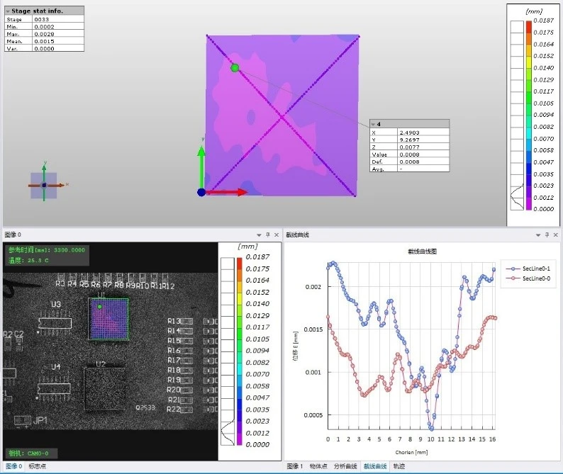
Out-of-Plane Displacement Analysis Along the Diagonal Section Line
Extract out-of-plane displacement data along the diagonal section line of the PCB:
|
Temperature
|
Maximum warpage along the diagonal cut line
|
Deformation features
|
|
Room temperature
|
0 μm(Benchmark)
|
Approximately straight
|
|
85℃
|
~15 μm
|
The center is raised, exhibiting a parabolic distribution.
|
|
125℃
|
~35 μm
|
The protrusion intensifies, and a slight depression appears at the margin.
|
|
Return to room temperature
|
~5 μm
|
Irreversible residual deformation; the distribution pattern is similar to that at high temperatures, but the magnitude is reduced.
|
Analysis Conclusion: PCB warpage increases non-linearly with rising temperature, and irreversible residual warpage persists after cooling back down from high temperatures; this indicates that the material is approaching its viscoelastic transition zone at 125°C.
IV. Summary of PCB Thermal Deformation Testing
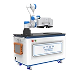
Using the XTOP3D XTDIC 3D full-field strain measurement system combined with a thermal stage, a "hardware isolation + software compensation + image enhancement" integrated thermal drift correction system was established. Through these technologies, the measurement accuracy of the microscopic DIC system regarding PCB thermal warpage was elevated to the micrometer level, meeting the rigorous demands for high-precision thermal deformation measurement in the field of electronic packaging.
1. Multi-level thermal drift correction technology system: A comprehensive technical scheme comprising "hardware isolation + software compensation + image enhancement" was developed. This controlled system thermal drift in high-temperature environments to the sub-micrometer level, overcoming the accuracy bottleneck of high-temperature microscopic DIC measurements.
2. Traceability of the full-process temperature history: Through stepped temperature control and synchronized image acquisition—combined with real-time drift correction—the true deformation data of the PCB across the entire cycle (room temperature → high temperature → room temperature) was fully recorded.
3. Quantitative warpage assessment capability: By analyzing displacements along diagonal cross-sections and employing single-point tracking, the magnitude of PCB warpage and residual deformation at various temperatures was precisely quantified, providing critical data support for the thermal reliability design of electronic products.
This technical scheme offers a reliable, precise, and scalable solution for high-temperature deformation measurement in fields such as electronic packaging, power devices, and MEMS, holding significant value for both engineering applications and academic research.