Over 50% of semiconductor component failures are caused by thermal stress concentrations and chip warpage resulting from thermal cycling. Traditional inspection methods—such as single-point probing, shadow moiré, and white-light interferometry—cannot meet the requirements for micron-level, full-field deformation measurement in advanced packaging; consequently, microscopic Digital Image Correlation (DIC) systems have emerged as the optimal, comprehensive solution.
Authoritative industry data indicates the following breakdown of causes for semiconductor component failure: temperature (55%), vibration (20%), humidity (19%), and dust (6%), making temperature-induced deformation the primary source of failure. With the widespread adoption of technologies such as 3D stacking, HBM, Fan-out, and QFN micro-packaging, significant mismatches in the Coefficients of Thermal Expansion (CTE) among multi-layer composite materials (silicon wafers, mold compounds, copper substrates, and solder balls) have become a critical issue. During processes like reflow soldering, high/low-temperature aging, and long-term powered operation, even micron-level warpage can trigger batch yield losses due to defects such as micro-bump cold joints, bridging, open circuits, delamination, and chip cracking.
I. Core Shortcomings of the Four Traditional Testing Solutions
1) Contact probes: can scratch the surface of microchips, can only collect data at a single point, and have no full-field strain data;
2) SM Shadow Moiré: It can only measure out-of-plane warping and cannot output in-plane displacement, XY strain, or CTE thermal expansion coefficient;
3) DFP digital stripe projection: In-plane measurement fails, strain accuracy is insufficient, and the microscopic field of view is poorly adapted.
4) WLI white light interferometry: Only local contour measurement is performed, and it is impossible to simultaneously obtain the three-dimensional displacement and strain distribution of the entire field.
II. Advanced Packaging and Testing: Three New Industry Challenges
First, miniaturization: the mainstream chip package size has been reduced to 1–10 mm, while the field of view of ordinary macroscopic DIC is too large to match the needs of microscopic observation;
Second, extreme temperature range: reflow soldering at 245℃ high temperature, liquid nitrogen at -190℃ low temperature, lens fogging under temperature difference, rigid displacement caused by thermal expansion of bracket, and interference of data by hot airflow refraction.
Third, dynamic full-process monitoring: Industry standards require continuous collection of deformation data throughout the entire process of heating, heat preservation, and cooling, while single-point snapshot measurement loses key transient warp peak values.
III. Microscopic DIC Measurement Scheme: Chip Thermal Deformation Process
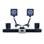
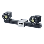
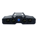
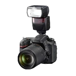
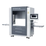
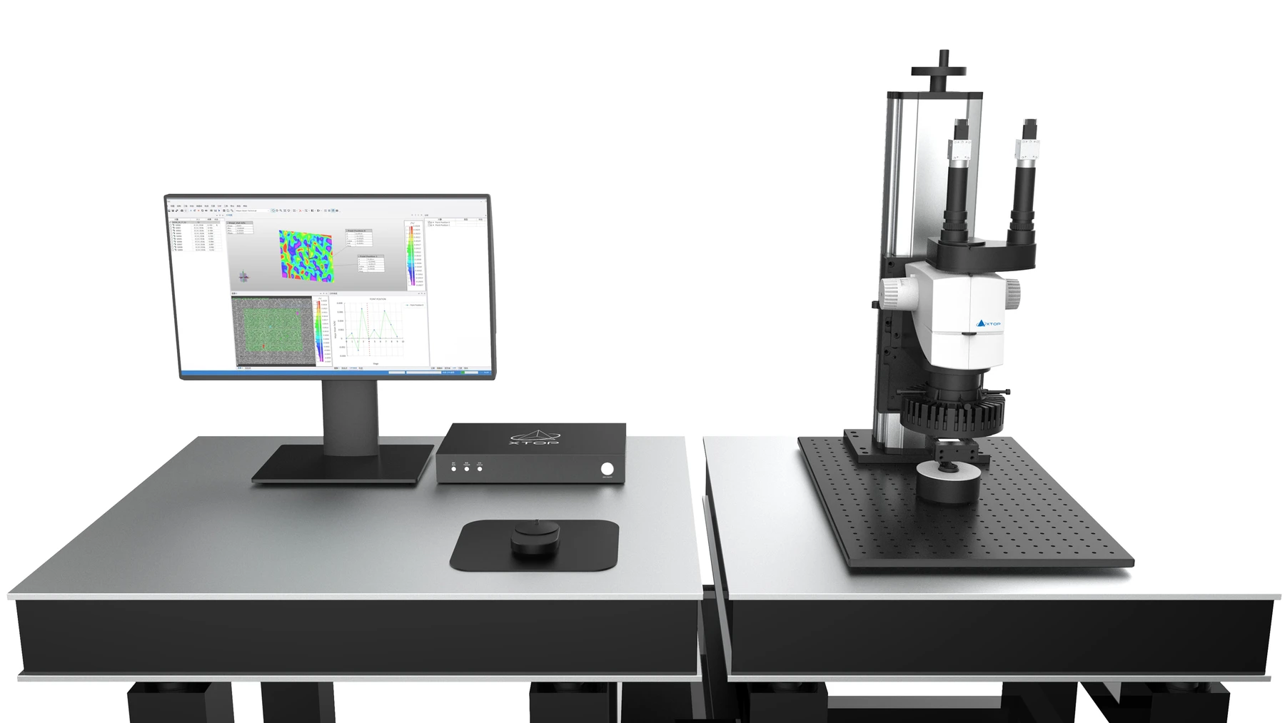
The Xintuo 3D Microscopic DIC Measurement System consists of three core modules: a binocular microscopic DIC measurement unit, a stereo microscope, and a programmable high-low temperature stage. It is specifically developed for the field of view of 1–10mm microchips and can achieve simultaneous measurement of warp, displacement, strain, and CTE in the full temperature range of -190℃ to 600℃.
3.1 Hardware Components List of the Microscopic DIC Measurement System
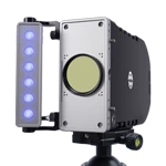
DIC measurement host: dual industrial cameras, ring stroboscopic light source, automatic microscopic calibration plate, sample spot preparation kit, XTOP three-dimensional analysis software;
Microscopic optical unit: 10x stereomicroscope, adapted for imaging of micro-packaged chips;
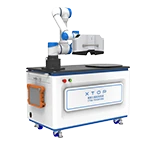
Temperature loading unit: Programmable hot and cold stage, supporting stepped heating, constant temperature holding, cyclic cooling, and thermal shock simulation;
Auxiliary components: vibration isolation workbench, sealed heat insulation cavity, anti-fogging circulating air duct.
IV. Core Advantages of Microscopic DIC Compared to Traditional Detection Techniques
DIC technology can simultaneously measure in-plane XY and out-of-plane Z full-field three-dimensional deformation, strain, and CTE. The other three mainstream detection technologies all have missing dimensions and cannot fully support the root cause analysis of chip failure.
3.1 Comparison of the full-dimensional capabilities of the four major optical inspection technologies
|
Measurable items
|
DIC Microscopy
|
SM Shadow Moore
|
DFP Digital Stripe Projection
|
WLI White Light Interference
|
|
Z-resolution
|
<0.5μm
|
<1μm
|
<10μm
|
<1μm
|
|
In-plane XY resolution
|
<1μm
|
No measurement capability
|
No measurement capability
|
No measurement capability
|
|
XY plane contour full field acquisition
|
support
|
Not supported
|
Not supported
|
Not supported
|
|
Z-direction out-of-plane displacement full-field acquisition
|
support
|
support
|
support
|
support
|
|
XY plane strain distribution
|
Full-view visualization
|
Unable to measure
|
Unable to measure
|
Unable to measure
|
|
Quantitative Calculation of CTE Thermal Expansion Coefficient
|
Native support
|
Not supported
|
Not supported
|
Not supported
|
|
Complete Warpage Warped Full Cloud Atlas
|
Full performance
|
Local finite measurement
|
Full performance
|
Local finite measurement
|
V. Microscopic DIC Measurement System: Solving Common Problems in the Microscopic High-Temperature Measurement Industry
Conventional macroscopic DIC applied to high and low temperature microscopic scenarios can lead to problems such as data drift, image blurring, and frost distortion. The Xintuo 3D Microscopic DIC Measurement System can effectively avoid measurement errors and ensure stable and reliable data under extreme temperatures.
1. Hot airflow suppression technology: isolates the refraction and scattering of rising airflow from hot and cold platforms, eliminates trend-based systematic errors, and results in a standard snowflake-like random data distribution;
2. Rigid displacement elimination technology: Automatically eliminates the overall displacement caused by the thermal expansion and contraction of the microscope support and the hot and cold stage, retaining only the actual warping deformation of the chip;
3. Fogging and frosting suppression technology: The sealed cavity is used for circulating temperature control and defogging, and the samples are clearly imaged throughout the high and low temperature process. There is no frost obstruction at a low temperature of -190℃.
4. Global temperature compensation algorithm: Automatically corrects pixel distortion in different temperature ranges, with no system offset in high and low temperature measurement data;
5. Automatic Microscopic Calibration Technology: One-click completion of microscope distortion calibration, eliminating manual calibration errors and significantly improving the repeatability of multiple measurements;
6. Super depth of field dynamic compensation technology: Automatic focus compensation for slight height shift of the sample during heating/cooling process, without losing the imaging depth of field throughout the process.
VI. Practical Application Value: Reducing Chip Failure and Yield Losses Across the Entire Supply Chain from R&D to Production Line
1. Research and development design stage: Calculate the CTE matching degree of different molding compounds, substrates and solder ball materials to avoid warping failure caused by CTE mismatch in advance;
2. Packaging process stage: Simulate the entire process of reflow soldering from 30℃ to 245℃ for heating and cooling, optimize the heating rate and holding time, and reduce micro-bump soldering defects;
3. Reliability verification phase: Complete the JESD22 temperature cycling aging test to quantify the cumulative deformation and stress concentration areas of the chip under long-term thermal shock;
4. Failure Analysis (FA): Precisely locates high-strain areas on chip cross-sections, corners, and pads, quickly pinpointing the root cause of batch failures and shortening the R&D iteration cycle.
VII. Industry FAQ
Q1: What is the difference between microscopic DIC and ordinary macroscopic DIC?
A: Macro DIC has a field of view of 50–500mm, suitable for large-size wafers; XDTIC-MICRO integrates a 10x microscope with a field of view of 1–10mm, submicron precision, and is equipped with a high and low temperature chamber, specifically adapted for thermal warpage testing of micro-packaged chips.
Q2: Can the equipment simulate the complete temperature profile of a real reflow soldering process?
A: Fully supported. The programmable hot and cold stages can be customized with stepped heating, constant temperature holding, and segmented cooling, replicating the standard reflow soldering conditions of 30℃/100℃/150℃/200℃/245℃. Data is collected after holding each temperature point for 5 minutes.
Q3: Can we simultaneously connect to finite element analysis (FEA) simulations for data benchmarking?
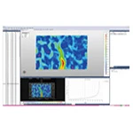
A: Our self-developed DIC software supports the import and comparison of FEA simulation data. The measured full-field strain cloud map can be directly compared with the simulation model to correct simulation parameters and improve the accuracy of chip structure design.
Q4: Is the equipment compatible with the stringent reliability testing of automotive-grade chips?
A: Temperature range from -190℃ to 600℃, meeting the full standard testing requirements for automotive-grade chips, including thermal shock, reflow soldering, and long-term high-temperature aging. Measurement data can be directly used for issuing third-party testing reports.
In the era of advanced packaging, micron-level thermal warpage of chips has become a core bottleneck restricting yield and reliability. Traditional single-dimensional inspection equipment cannot fully reproduce the entire deformation process. The micro-DIC measurement system , with its full-field three-dimensional synchronous measurement, sub-micron accuracy, full temperature range adaptability, and six anti-interference core technologies, can meet the full-dimensional inspection needs of chip thermal warpage, thermal deformation, strain, and CTE. It is the optimal standardized solution for semiconductor R&D, packaging and testing, and failure analysis laboratories.