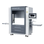
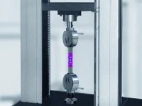
Microscopic DIC technology is essentially a fusion of binocular stereo vision and digital image correlation algorithms. By tracking random speckle patterns on the chip surface, it enables 3D reconstruction, pixel displacement tracking, and full-field strain calculation; it is the only optical measurement technique capable of non-contact, simultaneous output of 3D (XYZ) warpage and in-plane strain within a microscopic field of view.
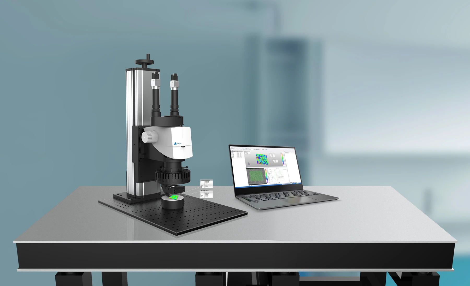
I. Introduction to Microscopic DIC Measurement System Technology
1.1 Principle of Binocular Stereo Vision 3D Reconstruction
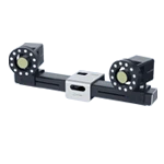
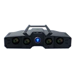
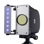
The microscopic DIC measurement system is equipped with two synchronous industrial cameras, forming a fixed baseline stereoscopic observation view. Combined with a 10x microscopic optical lens, it simultaneously captures speckle images of the chip surface. Based on a stereo matching algorithm, pixel matching is performed on the same speckle feature points of the left and right cameras. Combined with calibration parameters, the three-dimensional spatial coordinates of each feature point are calculated to construct a complete three-dimensional contour model of the chip surface. Unlike single-camera 2D planar measurement, the binocular approach can accurately capture Z-axis out-of-plane warpage (vertical bending deformation of the chip), which is the foundation for measuring chip thermal warpage.
Ordinary 2D cameras can only acquire planar displacement and cannot obtain the chip warp height difference; the micro-binocular DIC can output the Z-axis height of each micrometer point, with a minimum warp resolution of 0.5μm, perfectly matching the deformation measurement needs of QFN and CSP micro-packages.
1.2 Principle of Digital Image Correlation (DIC) Speckle Tracking Algorithm
Before testing, a uniform random speckle pattern is created on the chip surface as the unique feature identifier for the algorithm to track. The device acquires the original image at the reference temperature (room temperature) as a reference template; at each temperature node of heating and cooling, the sample image is captured simultaneously. The algorithm compares the speckle position offset of the two images pixel by pixel, calculates the X and Y plane displacement of each coordinate point, and further derives the Z-axis off-plane displacement by combining the binocular three-dimensional coordinates.
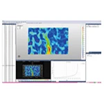
Based on the displacement gradient differential algorithm, the software automatically calculates the plane strain, principal strain, and shear strain of the entire field, and generates a visual strain cloud map to intuitively display the stress concentration areas at the four corners of the chip, the pads, and the substrate interface.
1.3 Core Differences Between Microscopic DIC and Conventional DIC
Conventional DICs lack optical magnification lenses and rely on wide field-of-view lenses to measure wafers and PCBs. Micro-DICs add stereo microscope optical magnification modules to reduce the effective measurement field of view to 1–10 mm. They are also equipped with micro-specific calibration algorithms, ultra-depth-of-field compensation, and a cold and hot anti-frost system to specifically solve the optical interference problem in the high and low temperature deformation measurement of micro-chips.
II. Microscopic DIC Measurement Technology: Standardized Chip Thermal Cycling Test Procedure
Conclusion: The entire chip thermal warp measurement system consists of five standardized steps: spot calibration, sample clamping, temperature profile programming, synchronous image acquisition, and data post-processing. The entire process is automated with minimal human intervention and high data reproducibility.
Step 1: Preparation of speckle patterns on the chip surface
A specialized speckle-making kit is used to spray uniform, random black and white speckles onto the surface of a 4–5 mm micro QFN chip. The speckle size matches the pixel resolution of the microscope lens, ensuring that the speckles do not fall off or fade at high temperatures, and meeting the requirements for long-term observation under high-temperature conditions of 245℃ reflow soldering.
Step 2: One-click automatic calibration of the microscope system
By placing a high-precision calibration plate specifically for microscopy, the software automatically completes the binocular camera distortion correction, microscope optical distortion compensation, and baseline parameter calibration, eliminating lens barrel distortion and magnification deviation, ensuring micron-level measurement accuracy, and eliminating the need for manual parameter adjustment throughout the entire process.
Step 3: Sample clamping and sealing of the high and low temperature chamber
Fix the chip to the hot and cold stage, close the heat insulation chamber, activate the anti-fogging circulating air duct, pre-cool/preheat the chamber to eliminate temperature difference airflow within the chamber, and avoid lens frost and airflow refraction interfering with the image during the test process.
Step 4: Loading programmable temperature curve + synchronous image acquisition
The system replicates the industry standard reflow soldering temperature profile: 30℃ room temperature for 5 minutes → 100℃ for 5 minutes → 150℃ for 5 minutes → 200℃ for 5 minutes → peak temperature of 245℃ for 5 minutes, then cools down in stages back to room temperature; the system automatically triggers dual cameras to capture images at each constant temperature node, with no manual interruption throughout the process.
Step 5: 3D Deformation Data Analysis using DIC Software
DIC software automatically completes speckle matching, 3D reconstruction, and displacement-strain calculation, and outputs with one click: 2 warpage contour maps, Z-axis warpage numerical curves, cross-sectional deformation polygons, full-field strain distribution, CTE thermal expansion coefficient, and temperature-warpage corresponding data tables. It also supports data export and integration with FEA simulation software.
III. Self-developed micro-DIC technology solves the challenges of microscopic high and low temperature measurement and testing.
High-temperature microscopic measurements of chips have common sources of measurement error that conventional DIC equipment cannot address. Newtop 3D has developed a dedicated algorithm and hardware structure to eliminate these systematic errors one by one.
3.1 Principle of Hot Airflow Suppression Technology
The heating of the hot and cold stages generates rising hot airflow. Changes in air density gradient cause light refraction, resulting in a regular shift in the speckle image and ultimately leading to systematic data distortion. The equipment incorporates a built-in annular sealed air duct, with constant-temperature circulating airflow isolating the hot and cold stages from thermal convection, ensuring uniform air refractive index in the optical path, eliminating trend-based measurement errors, and reducing data error to within 0.5μm.
3.2 Principle of Rigid Displacement Elimination Technology
During the heating process, the hot and cold stage support and microscope base will expand and contract synchronously due to thermal changes, resulting in overall rigid translation. The software may mistakenly identify the device's own displacement as chip deformation. The algorithm automatically separates the rigid displacement component of the device from the actual local deformation component of the chip by matching global reference points, retaining only the chip's own warpage data, thus solving the measurement distortion caused by the thermal expansion of the support at high temperatures.
3.3 Principle of Fogging and Frosting Suppression Technology
At low temperatures of -190℃ and liquid nitrogen, water vapor condenses inside the chamber, forming frost and fog on the lens and sample surfaces, obscuring speckle patterns. At high temperatures above 200℃, water mist forms due to the temperature difference. The system is equipped with a constant-temperature drying and circulating air duct that continuously replaces the chamber with dry nitrogen, keeping the lens and sample free of fog and frost throughout the high and low temperature process, ensuring clear and stable image acquisition.
3.4 Principle of Global Temperature Compensation Algorithm
The refractive index of an optical lens changes slightly at different temperatures, causing pixel coordinate drift. A built-in multi-temperature calibration database automatically calls the corresponding correction parameters based on the real-time hot and cold stage temperatures, dynamically correcting image distortion and ensuring stable measurement accuracy across the entire temperature range.
3.5 Principles of Automatic Microscopic Calibration Technology
Traditional manual microscope calibration relies on manual focusing, and even slight deviations in magnification can lead to micron-level data distortion. This system employs a backlit photolithographic calibration plate, with software automatically identifying calibration point coordinates and fully automatic correction of microscope distortion. Repeatability errors after multiple measurements are ≤0.5μm.
3.6 Principle of Hyper-Depth of Field Dynamic Compensation Technology
Chip heating causes Z-axis warping, which extends beyond the microscope's fixed depth of field, resulting in image blurring. The algorithm monitors the sample surface speckle sharpness in real time and automatically fine-tunes the microscope's focusing height, ensuring the sample remains within the effective depth of field throughout the process, preventing image defocusing and data loss.
IV. Analysis of Microscopic DIC Measurement System and Application Logic of Chip Failure
The micro-DIC measurement system can output quantitative data in one go, and locate the root cause of chip thermal warping failure from multiple dimensions such as contour, displacement, strain and thermal expansion coefficient. A single device can replace multiple traditional testing instruments.
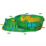
1. 3D contour cloud map: Intuitively visualize the overall bowl-shaped/saddle-shaped warping shape of the chip and determine whether the symmetrical deformation meets the packaging design expectations;
2. Z-axis warpage value: Extract the maximum warpage height of the chip center, four corners and pads, and quantify whether the micron-level deformation exceeds the process standard threshold;
3. Full-field XY plane displacement field: Observe the stretching, contraction, and displacement of the chip plane to determine the slippage at the interface between the substrate and the chip;
4. Two-dimensional/three-dimensional strain distribution cloud map: accurately marks areas of high strain concentration, and locates risk points of chip cracking, delamination, and solder joint breakage;
5. Coefficient of thermal expansion (CTE): Quantitatively calculates the coefficient of thermal expansion of the chip, molding compound, and substrate to determine the degree of CTE mismatch in multilayer materials;
6. Temperature-Deformation Timing Curve: Fully records the warp changes throughout the entire process of heating, holding, and cooling, capturing the peak temperature and maximum deformation inflection point during reflow soldering.
V. The Differentiated Technological Value in Scientific Research and Industrial Scenarios
5.1 University/Materials Research Scenarios
It can be used to conduct fundamental research on the thermodynamics of micro-semiconductor materials, calculate the CTE parameters of novel molding compounds and packaging substrates, and verify the thermal stress coupling mechanism between chip layers. It is a standard measurement device for microelectronics and materials mechanics laboratories.
5.2 R&D/Failure Analysis Scenarios for Packaging and Testing Companies
Rapidly complete reflow soldering simulation and temperature cycling aging tests, compare warpage differences of different packaging structures and filling materials in batches, and shorten the R&D and verification cycle of new chips; perform FA failure tracing for batches of cold solder joints and delamination failure samples to accurately locate the root cause of thermal stress concentration.
VI. Technical Popular Science FAQ
Q1: Will microscopic DIC measurement damage the chip sample?
A: Completely non-contact optical measurement, without probes or mechanical contact, will not scratch the pads of microchips or the surface of plastic packaging, and can perform non-destructive and repeatable testing of expensive automotive-grade chips and R&D samples.
Q2: Will the speckle pattern detach at a high temperature of 245℃, affecting the measurement?
A: It comes with special high-temperature resistant spot-forming consumables that can maintain the temperature at reflow soldering temperatures below 260℃ for a long time without peeling or fading, meeting the standard reflow soldering full process test.
Q3: Can a conventional DIC test microchips?
A: It cannot be achieved. Without an optical magnifying lens, the pixel resolution is insufficient, and speckle on the surface of 1–10mm microchips cannot be effectively identified. The warpage accuracy can only reach the micrometer level or above, which cannot meet the μm-level measurement requirements.
Q4: Can the DIC algorithm distinguish between rigid displacement of the device and actual deformation of the chip?
A: Relying on rigid displacement elimination, the patented algorithm automatically separates the two displacement components, eliminating the need for manual deduction of the reference, and automatically filtering the data to remove interference caused by the thermal expansion of the equipment.
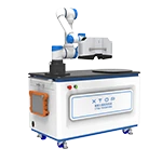
The microscopic DIC measurement system, based on binocular stereo vision and digital image correlation algorithms, and incorporating six proprietary anti-interference technologies, solves the industry pain point of three-dimensional full-field thermal warpage and strain measurement of microchips under high and low temperature environments. The Xintuo 3D microscopic DIC measurement system integrates microscopic optical magnification, high and low temperature loading, automated calibration, and multi-dimensional data post-processing into a unified solution. It completely reproduces the micron-level deformation law of the chip from room temperature to the reflow soldering peak temperature, and is a standardized optical measurement technology for thermodynamic testing and failure analysis of advanced semiconductor packaging.