In practical applications, electronic components are often exposed to environments characterized by significant temperature fluctuations. Temperature cycling tests subject components to repeated, rapid transitions between high and low temperatures; this process exposes and allows for the elimination of failures caused by issues such as mismatched thermal expansion coefficients between materials, mismatches in temperature coefficients between internal leads and die coatings, chip cracking, poor contact, or manufacturing defects.
Due to the small size of electronic components, contact-based measurement methods are unsuitable; instead, optical non-contact measurement solutions are required to analyze deformation behavior under high and low-temperature conditions. To ensure product reliability and longevity under high-temperature operating conditions, a leading telecommunications equipment manufacturer adopted the XTOP3D XTDIC-MICRO 3D microscopic strain measurement system. This system enables non-contact, full-field, high-precision deformation monitoring and analysis, helping engineers optimize material selection and thermal management designs while enhancing overall product reliability.

Deformation of Electronic Components Under High and Low Temperatures and Its Consequences
In high-temperature environments, disparities in the coefficients of thermal expansion (CTE) among materials within electronic components can lead to internal stress concentration, triggering the following issues:
CTE Mismatch: Differences in thermal expansion coefficients between materials (such as the chip, packaging, and substrate) generate shear stress at interfaces;
Micro-cracks and Delamination: Prolonged exposure to high temperatures can cause micro-cracks to form between the packaging layer and the chip, impairing electrical performance;
Mechanical Structural Failure: Repeated deformation of structures—such as packaging housings and wire bonds—during thermal cycling can lead to fatigue failure;
Reduced Reliability: High temperatures accelerate material aging, shorten product lifespan, and compromise the stability of the entire system.
If these issues are not identified during the design phase, they can lead to product failure during actual use, resulting in significant economic losses and safety hazards.
Test Objectives
Evaluate the 3D strain distribution and deformation trends of electronic components in high-temperature environments;
Quantitatively analyze the strain evolution of the packaging structure during thermal cycling;
Identify potential stress concentration zones and early-stage failure mechanisms;
Optimize material selection and structural design to enhance high-temperature product reliability;
Provide data support for the formulation of reliability assessment standards for components.
Testing Procedure
An optical heating/cooling stage (temperature range: -190°C to 600°C; customizable) is integrated with an optical DIC microscope system to conduct in-situ variable-temperature testing.
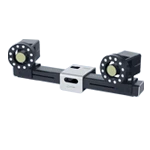
XTOP3D XTDIC-MICRO 3D microscopic strain measurement system (includes tools for applying speckle patterns to micro-scale materials and a fully automated calibration turntable for one-click automated calibration).
Test steps
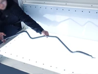
Sample marking: Prepare speckle patterns on the surface of electronic components and place them on hot and cold stages to facilitate high and low temperature environment simulations.

Adjustment of the microscopic DIC system: Based on the size of the specimen, a 1× magnification is selected for the stereo microscope, and the same 1× magnification is used for the calibration plate, as shown in the figure.

Micro-DIC system calibration. The XTOP3D XTDIC-MICRO 3D microscopic strain measurement system utilizes a fully automated calibration turntable to enable one-click, automated calibration. By calibrating the internal and external camera parameters, the system accurately acquires 3D data of the test specimen.


Temperature ramping and data acquisition. The heating and cooling rate was 10°C/min; the temperature was raised from 25°C to 300°C, held constant for a period, and then lowered to 25°C. This cycle was repeated three times, with the XTDIC-MICRO 3D microscopic strain measurement system capturing images at a rate of one frame every 6 seconds.


Micro-DIC System Test Results
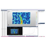
Within the XTOP3D DIC software, the speckle region was selected and seed points were added to calculate the specimen's deformation data across varying temperatures; the images below illustrate the results at 25°C, 50°C, 100°C, 200°C, and 300°C, respectively.
3D Strain Distribution Map: Clearly reveals significant strain concentration on the surface of the component specimen under high-temperature conditions.
Thermal Cycling Strain Evolution Curve: Demonstrates rapid strain accumulation during the high-temperature phase and partial strain recovery during the low-temperature phase.
Failure Mechanism Analysis: Identifies regions of strain concentration and peak strain values under high-temperature conditions, helping to prevent failures caused by issues such as mismatched thermal expansion/contraction properties, mismatched coefficients of thermal expansion between internal bonding wires and die coatings, and chip cracking.


By selecting key deformation points on the electronic component specimen, strain curves varying with the time history can be plotted:

Analyze the change in distance between two points and obtain the change in deformation spacing between them:

Value to Manufacturers
Enhances product reliability: Prevents large-scale failures in later stages by identifying high-temperature deformation issues early;
Shortens R&D cycles: Rapidly acquires deformation data, reducing costs associated with trial and error;
Strengthens competitive advantage: Meets the industry's growing demand for highly reliable components;
Improves testing efficiency: Utilizes non-contact, automated testing processes to save time and labor.
Expanded Applications
The XTOP3D XTDIC-MICRO 3D microscopic strain measurement system is suitable not only for testing the thermal deformation of electronic components but also for a wide range of applications in the following fields:
- Chip thermal expansion/warpage analysis: Analyzing warpage distribution and the coefficient of thermal expansion (CTE) of chips under high and low-temperature conditions.
- Single-crystal silicon CTE measurement: Evaluating the CTE of single-crystal silicon across various temperature environments.
- PCB thermal expansion testing: Analyzing micro-displacements and strain in PCBs at different temperatures.
- Semiconductor packaging analysis: Evaluating the deformation of packaging materials in high-temperature environments.
- 5G equipment and server motherboards: Investigating the thermal stability of high-speed circuits and optimizing signal integrity.
- New energy vehicle battery management: Measuring battery thermal expansion and optimizing cooling solutions.
- Aerospace composite material research: Evaluating the thermal expansion and deformation characteristics of materials subjected to extreme temperature variations.