Thermal loading is the primary stress factor during wafer processing and operational service. A mismatch in the coefficients of thermal expansion (CTE) among multi-layered materials generates thermomechanical stress, leading to wafer warpage—which can directly cause cracks, open circuits at solder joints, electrical shorts, and device performance failure.
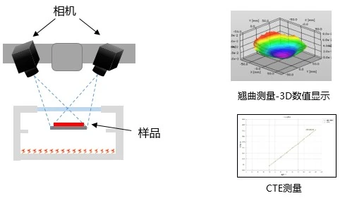
Digital Image Correlation (DIC) technology enables the capture of full-field 3D topography, displacement, and strain across the entire temperature range. It provides empirical, quantitative data essential for process optimization, thermal matching in packaging, and the reliability certification of semiconductor chips.
01. Why do wafers warp? What is the cost of such warpage?
A wafer is a multi-layered, heterogeneous material stack. Its constituent components—the silicon substrate, dielectric thin films, and subsequent packaging materials—possess different coefficients of thermal expansion (CTE). When the temperature changes, these layers exhibit varying tendencies to expand or contract; however, because they are bonded together, they are constrained and cannot deform independently. This leads to the accumulation of internal thermo-mechanical stress, which is ultimately released through warpage.
Reference values for the CTE of common semiconductor materials:
|
Material layer
|
Typical CTE(ppm/°C)
|
|
Silicon waferc
|
2.6~3.0
|
|
Epoxy Molding Compound (EMC)
|
8~15
|
|
Substrate BT/ABF
|
12~17
|
|
Solder SAC305
|
21~25
|
|
Copper Interconnect/Lead Frame
|
16~17
|
Warpage is more than just a visible deformation; it propagates throughout the entire chain—encompassing manufacturing, reliability, design, and testing—and incurs a fourfold cost:
|
Dimension
|
Actual impact
|
|
Manufacturing and Packaging
|
Component misalignment, "pillow effect," bridging, and cold/open solder joints—leading to a collapse in yield rates and a sharp surge in production costs.
|
|
Device Reliability
|
Chip cracking, interfacial delamination, and solder joint fatigue; premature device failure and a significant reduction in service life.
|
|
Design Constraints
|
By altering the interconnect and thermal management configuration, the upper limits for both electrical and thermal performance of the package are effectively locked in.
|
|
Testing and Verification
|
Measuring full-field, micron-scale deformation within a high-temperature, enclosed chamber is highly challenging, and single-point measurement methods are incapable of capturing the risks associated with localized deformation.
|
02. Why choose 3D DIC for measuring warpage?
|
Method
|
What can it measure?
|
Typical Scenarios
|
|
Shadow Moiré
|
Z-direction warpage
|
Mass-production sampling inspection, rapid flatness assessment
|
|
DFP
|
Z-axis warpage, large field of view
|
Panel/Wafer Inspection
|
|
3D-DIC
|
Full-field displacement + strain + CTE + warpage
|
R&D, failure analysis, and simulation benchmarking
|
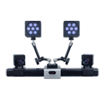
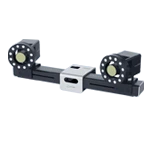
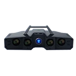
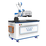
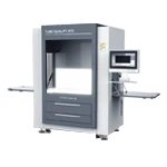
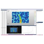
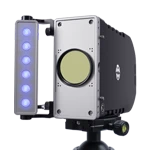
The XTOP3D XTDIC 3D strain measurement system provides simultaneous output for warpage topography, full-field displacement, strain fields, and CTE (Coefficient of Thermal Expansion) data. It is well-suited for R&D iteration, failure analysis, and simulation benchmarking.
Applicable samples include silicon wafers, packaged wafers, BGAs, substrates, and thin-film frames. Measured parameters include warpage, coplanarity, full-field strain, and the coefficient of thermal expansion (CTE).
03. Practical Case Study: Thermal Warpage Testing of a Wafer (0°C–150°C)
Test Objective: To replicate the evolution of wafer warpage throughout the heating process, quantify out-of-plane displacement amplitudes at various temperatures, and identify localized regions of concentrated deformation, thereby providing empirical data for thermal matching in packaging.
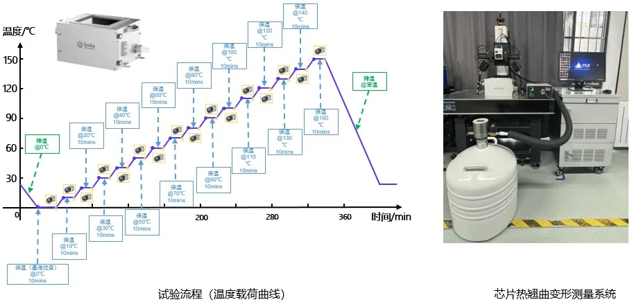
The sample is a 6-inch single-crystal silicon wafer (150 mm in diameter, 1 mm thick). The test covers a temperature range of 0°C to 150°C, employing a stepped isothermal approach with increments of 10°C—comprising 16 temperature nodes (S₀–S₁₅). The setup utilizes an XTDIC 3D strain measurement system integrated with a high-low temperature test chamber.
Temperature-Load Profile and DIC-Based Thermal Warpage Testing System
Test Results and Interpretation
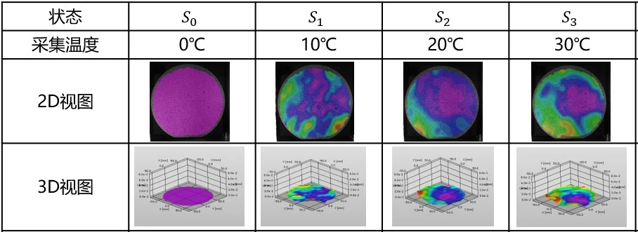
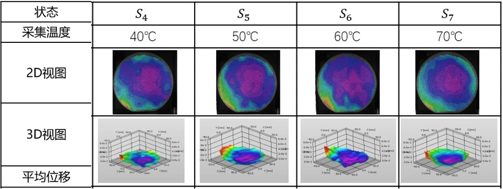
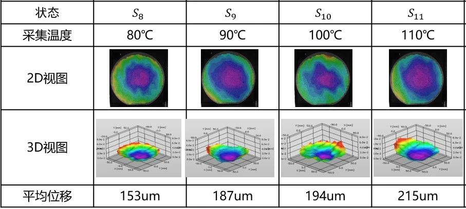
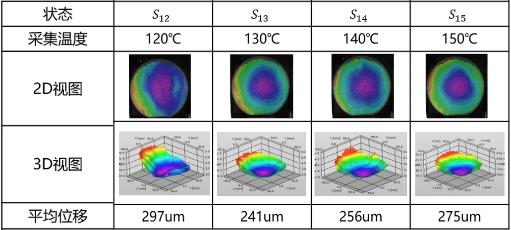
Wafer warpage is a form of non-uniform deformation, with significant variations observed across different regions.
As the temperature rises, the overall warpage continues to increase; at 120°C, the average out-of-plane displacement reaches 297 μm, marking the peak for this heating phase. As the temperature rises further, stress within the silicon material is released, causing the magnitude of the warpage to decrease slightly rather than continue to grow.
2D/3D thermal warpage results for the S0–S3 temperature ranges
2D/3D thermal warpage results for the S4–S7 temperature range
2D/3D thermal warpage results for the S8–S11 temperature range
2D/3D thermal warpage results for the S12–S15 temperature range
04. Proprietary DIC Algorithms Enabling Precise Test Data
When it comes to wafer warpage testing, the rule is simple: if you cannot measure it, you cannot control it; and if your measurements are inaccurate, it is as if you never measured it at all. High-precision DIC-based thermal warpage and deformation testing relies fundamentally on the proprietary DIC algorithms developed in-house by XTOP 3D.
|
Self-developed algorithms
|
Technical Capabilities and Value
|
|
Sub-pixel speckle analysis algorithm
|
Out-of-plane measurement accuracy < 0.5 μm, in-plane measurement accuracy < 1 μm
|
|
Rigid-Body Displacement Elimination Algorithm
|
Eliminate the interference of overall rigid-body motion to preserve the true deformation field of the wafer.
|
|
Window Refraction Calibration Technology
|
Correction of refractive distortion to ensure measurement accuracy
|
|
Temperature-Graph Synchronous Correlation Algorithm
|
Image matching mapped to temperature nodes; analysis of deformation evolution across the full temperature range.
|
|
Full-field post-processing analysis algorithm
|
3D Warpage/CTE Thermal Expansion, Full-Field Strain Maps
|
Unlike single-point measurement, XTOP3D’s DIC (Digital Image Correlation) technology enables the full-field reconstruction of deformation evolution across an entire temperature profile. It allows for the quantification of warpage, the capture of localized deformations, and the assessment of thermal matching in heterogeneous materials. By providing critical experimental data for refining packaging processes, selecting materials, and verifying reliability, this technology helps reduce the risk of chip-soldering failures.