I. Overview
Printed Circuit Boards (PCBs) serve as the fundamental carriers for electronic devices, providing both electrical interconnections and mechanical support for components. They are widely used in products such as mobile phones, computers, and wearable electronics. During processes like reflow soldering or operation in environments with fluctuating temperatures, mismatches in the Coefficient of Thermal Expansion (CTE) between the PCB and its components can lead to thermal warpage. This, in turn, often results in reliability issues such as solder joint fatigue, connection failures, component cracking, and component displacement.
Traditional measurement methods are limited to capturing data at discrete points, while conventional Digital Image Correlation (DIC) techniques are often compromised by factors like air refraction caused by heat, thermal radiation, and thermal drift in the testing fixtures, leading to distorted measurement data. This solution utilizes the XTOP3D XTDIC 3D strain measurement system—based on Digital Image Correlation (DIC) technology—which incorporates a comprehensive thermal drift correction framework combining hardware isolation, software compensation, and image enhancement. This enables non-contact, full-field, micron-level warpage measurement of PCBs under thermal loading, providing quantitative experimental data to support the thermal reliability design of PCBs.
II. Testing Requirements and Technical Challenges
Testing Requirements
1. Capture the full-field, three-dimensional deformation of the PCB throughout the entire thermal cycle—including heating, isothermal holding, and cooling phases.
2. Quantify the maximum warpage/deflection, localized bulges or depressions, and residual permanent deformation of the PCB at various temperatures.
3. Distinguish between the rigid-body displacement caused by the test fixture and the actual, intrinsic deformation of the PCB.
4. Evaluate the viscoelastic creep behavior of the PCB at high temperatures; the capability to measure the coefficient of thermal expansion (CTE) of the board material should also be supported.
Bottlenecks in Conventional DIC Technology Applications
1. Interference from Hot Air Turbulence and Refraction: In high-temperature environments, thermal convection and temperature gradients cause non-uniform air refractive index distribution. This results in "apparent" or "noise-induced" displacements in the captured images, directly leading to distorted calculations of strain and warpage.
2. Multiple Errors Introduced by Thermal Environments: High-temperature thermal radiation can degrade the performance of speckle coatings, while cameras and lenses may experience thermal drift. Furthermore, the use of protective heat-insulating glass introduces optical refraction distortion, which further amplifies image-matching errors.
3. Displacement Ambiguity Due to Thermal Expansion and Contraction of Fixtures: During heating or cooling cycles, fixtures and mounting stages undergo thermal expansion or contraction. Conventional DIC lacks specialized algorithms to distinguish between the rigid-body displacement caused by this tooling and the actual deformation of the PCB.
III. Composition of the DIC Thermal Deformation Testing System
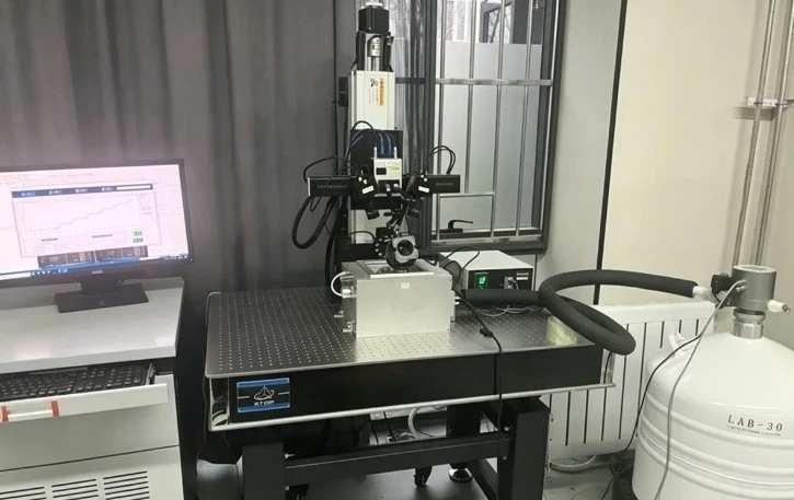
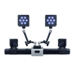
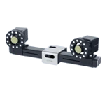
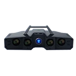
The XTOP3D XTDIC 3D strain measurement system incorporates core algorithms for distortion correction, automatic rigid-body displacement removal, and thermal drift compensation. Temperature control is achieved via an optical heating/cooling stage, covering a range from room temperature to 125°C with a precision of ±0.5°C. The system features an actively temperature-controlled quartz glass viewing window and a closed-loop cooling system, ensuring the surface temperature of the window remains below 50°C.
The XTDIC 3D strain measurement system is equipped with a high-temperature-resistant speckle-pattern preparation kit, an LED cold light source paired with a narrow-band optical filter, ceramic reference blocks, and a vibration-isolated optical table. The complete system exhibits a thermal drift error of less than 0.5 μm and a single-point displacement standard deviation of less than 0.3 μm.
IV. Typical Application Cases
Case 1: Warpage and Deformation Testing of PCB Circuit Boards Under Thermal Loading (Thermal Cycling from Room Temperature to 125°C)
Test Procedure
A high-temperature-resistant speckle pattern is applied to the surface of the test specimen. The PCB is placed on a support frame within a thermal chamber, where ceramic reference points are positioned to facilitate thermal drift compensation. The binocular Digital Image Correlation (DIC) system is calibrated at room temperature, with a pre-calibration step performed to account for thermal drift; a cold light source is also adjusted to optimize image quality.
Temperature control follows a stepped thermal cycle: room temperature (baseline) → hold at 85°C → hold at 125°C → return to room temperature. At each temperature stage, image acquisition is initiated only after the temperature fluctuations within the chamber are stabilized to within ±0.5°C. The binocular DIC cameras capture multiple frames synchronously, which are then averaged to reduce noise. Finally, the DIC software outputs 3D deformation field data, corrected for thermal drift.
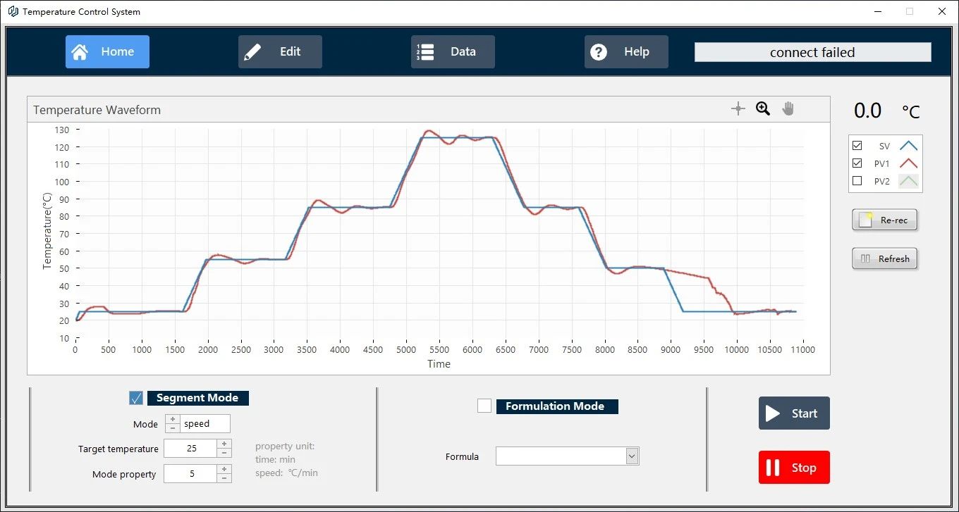
温度控制曲线界面
Test Results and Analysis
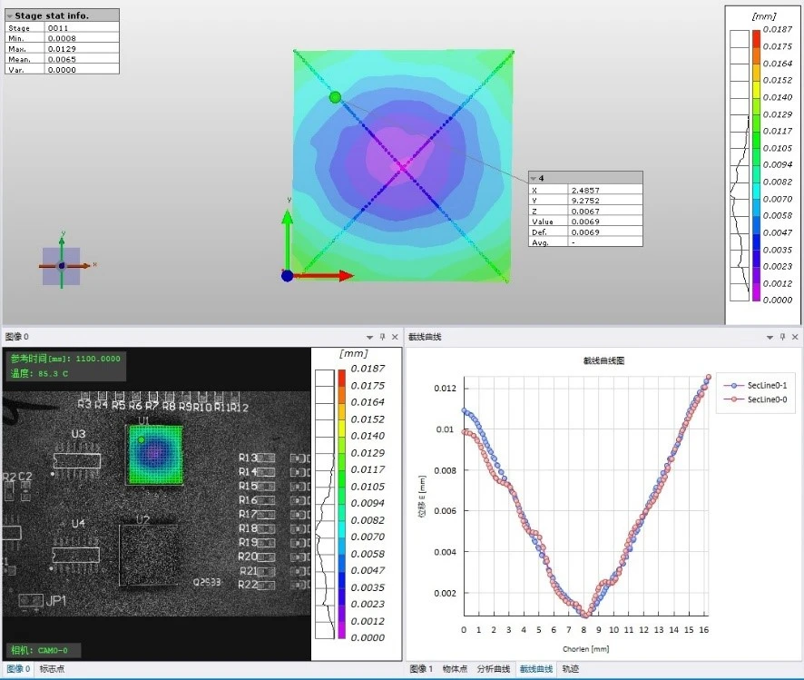
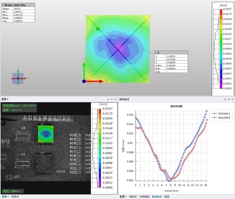
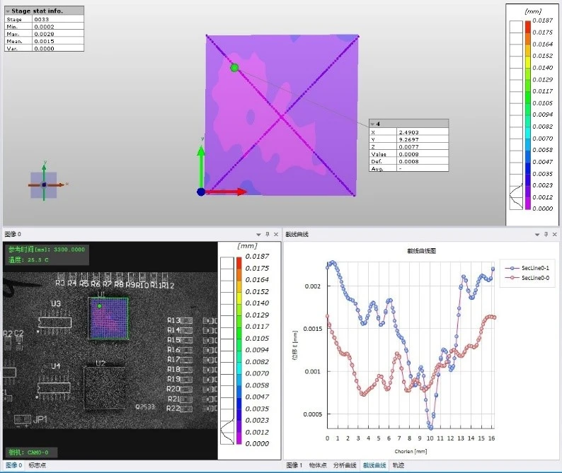
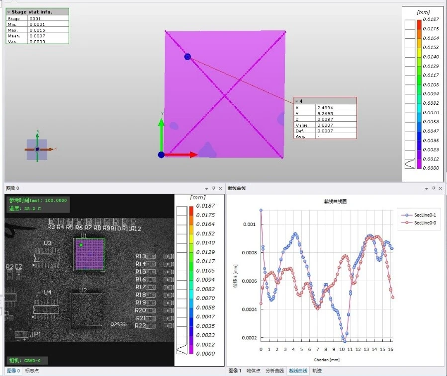
Full-field 3D topography, out-of-plane displacement contour maps, and displacement profiles along diagonal cross-sections were acquired for the PCB under four conditions: baseline room temperature, 85°C, 125°C, and after returning to room temperature.
(1) Baseline Room Temperature (Zero-Displacement Reference State)
At room temperature, the PCB is generally flat. Serving as the zero-displacement reference, the standard deviation of displacement at any single point is <0.3 μm.
(2) At a constant temperature of 85°C
Thermal expansion leads to warping, with the central region of the circuit board bulging into a bowl-like shape; the maximum warpage along a diagonal cross-section is approximately 15 μm.
(3) Condition during isothermal holding at a maximum temperature of 125°C
Warpage reaches its peak, with the central bulge becoming more pronounced; the maximum warpage is approximately 35 μm. The edges of the board, being constrained, exhibit a slight, inverse inward curvature (concavity).
(4) Cooling back to room temperature
Most of the thermal deformation recovers, but a residual deformation of approximately 5 μm remains in the central region; this indicates that viscoelastic creep occurred in the PCB substrate at high temperatures, resulting in irreversible warpage.
Experimental results indicate that the warpage of PCB boards increases non-linearly with rising temperature; at 125°C, the material approaches its viscoelastic transition range. Upon cooling back to room temperature, a residual warpage of approximately 5 μm remains—a deformation that increases the risk of solder joint failure and component placement misalignment. Through the extraction of diagonal cross-sectional profiles and the analysis of full-field contour maps, it is possible to intuitively locate areas of PCB bulging or depression, thereby elucidating the underlying mechanisms by which high-temperature warpage induces component placement misalignment.
Case 2: PCB board thermal expansion and expansion and contraction performance test under high and low temperature impact
Test process
The XTDIC three-dimensional strain measurement system, combined with a programmable constant temperature and humidity testing machine, can carry out wide temperature range temperature impact testing on PCB samples. The test temperature range is set to ‑40℃~100℃. Each 10℃ increase is regarded as a test stage. Each temperature stage is kept warm for 5 minutes, for a total of 15 temperature conditions.
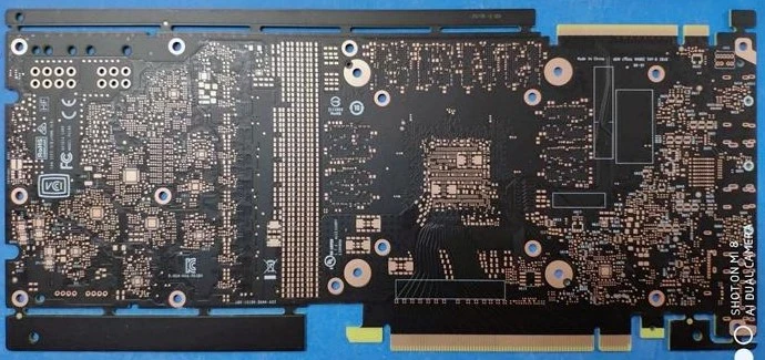
Prior to testing, a high-temperature-resistant speckle pattern is applied to the specimen, and the 3D Digital Image Correlation (DIC) strain measurement system is calibrated. Once the temperature has stabilized for each specific test condition, images are captured synchronously. The DIC system tracks point-by-point displacements on the PCB surface across horizontal, vertical, and diagonal directions. By calculating the full-field displacement and strain distributions at various temperatures, the coefficients of thermal expansion (CTE) of the PCB in different directions are determined.
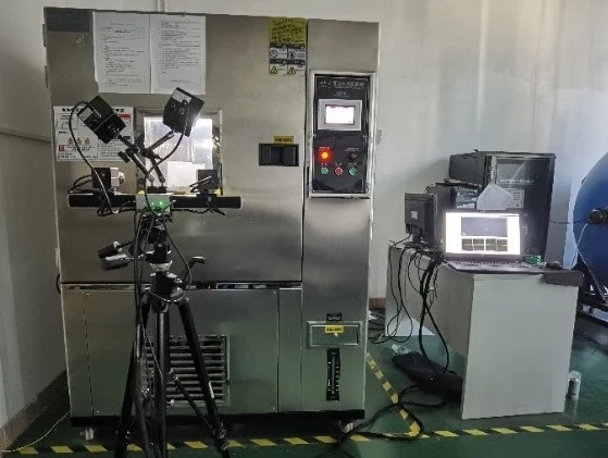
On-site high-low temperature shock DIC testing
Test Results and Analysis
Temperature parameters of the testing machine were recorded throughout the test process, covering the entire test range from -40°C to 100°C.
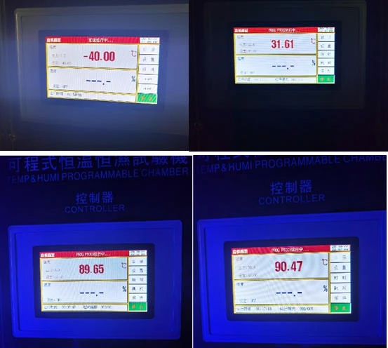
Temperature display interface for each stage
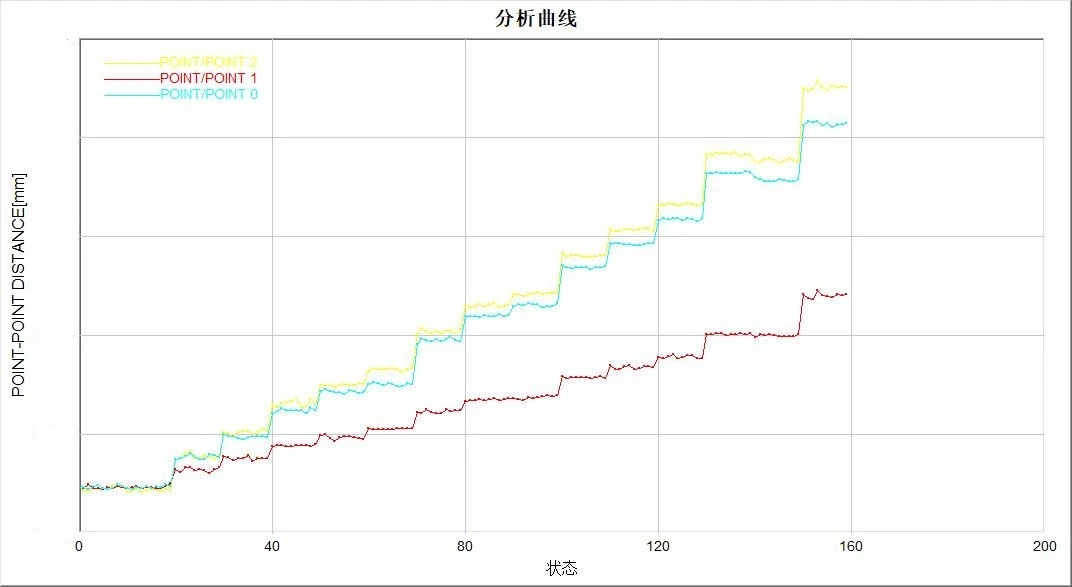
The DIC software tracks feature points on the PCB specimen in the horizontal, vertical, and diagonal directions, and outputs curves showing the variation of point-to-point distances as a function of test conditions.
DIC technology enables the acquisition of full-field displacement and strain data, providing a comprehensive visualization of deformation distribution across a PCB surface and identifying localized regions of strain concentration. By analyzing changes in length and relative displacement at various temperatures, it is possible to quantify the coefficients of thermal expansion (CTE) for PCBs and evaluate residual thermal stresses resulting from the lamination process of multilayer boards. This provides critical experimental data for selecting PCB laminates and optimizing high-density, advanced-layer PCB manufacturing processes, helping to preemptively mitigate the risk of product scrap caused by unexpected expansion or shrinkage.
V. Test Summary and Application Value
Digital Image Correlation (DIC) technology can be used to characterize material parameters such as Young’s modulus, Poisson’s ratio, glass transition temperature ($T_g$), and the coefficient of thermal expansion (CTE), making it highly valuable for evaluating candidate materials for PCB laminates. A mismatch in the CTE between a chip package and a PCB can lead to thermo-mechanical damage at the interface, which in turn induces solder joint fatigue. By measuring the CTE of PCBs and electronic components, one can effectively identify the risks of solder joint fatigue caused by thermal cycling.
During the reflow soldering process, warpage in PCBs and components can easily result in failures such as poor connections, solder bridging, and component cracking. A warpage testing solution based on DIC technology not only detects warpage issues during reflow soldering but also enables the comparative evaluation of the performance of candidate components and PCB laminate materials.
This solution utilizes the XTDIC 3D strain measurement system, which incorporates a three-pronged thermal drift correction approach—combining hardware isolation, software compensation, and image enhancement—to overcome the limitations of conventional DIC measurements in high-temperature environments. It enables non-contact, full-field deformation detection at the micron scale. The testing process can fully replicate the deformation of a PCB across its entire operating temperature range, providing key metrics such as warpage magnitude, residual deformation, and the coefficient of thermal expansion. These data support the proactive assessment of risks—such as solder joint failure or BGA placement offset—thereby guiding the thermal reliability design of PCBs and reducing product defect rates.








 Video Center